output capacitor selection or removal??
1. The audio express article i referenced above recommends a 1000 uF cap at the output of the voltage regulators. Initially i though it was to reduce the output impedance of the supply at higher frequencies (10-20 khz = high, it is an audio power supply after all) as described in this article:
Understanding Power Impedance Supply for Optimum Decoupling
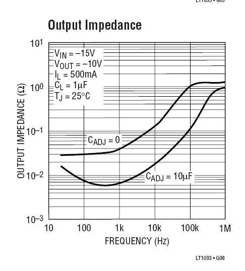
However, based on the data sheet output impedance specs for the LT1033 (shown below), it seems clear that there isn't a cap that can reduce the output impedance over the audio band. Any cap with a high enough capacitance would have an ESR that is much greater than the max impedance in the audio band (0.02 ohm max, with adjust coupling cap). The smaller value caps with much lower esr all have too much reactance in the audio band to lower output impedance there.
My first question is: What is the purpose of the output cap? Since it can't lower the output impedance in the audio band is it only there to filter, if so what would be a good value capacitance to choose? Is any additional filtering after the regulator really necessary (i'm using a 2 stage filter before the regs, only 1 is on the pcb). Alternatively, should i just omit the cap because having higher output impedance at frequencies above the audio band is possibly advantageous?
My second question is about the effect of the adjust pin bypass cap on output impedance. On clear advantage of the adjust pin bypass cap is that it lowers the output impedance, however, it also makes the impedance profile less flat. Might it be better to accept the higher output impedance (0.03 ohm vs about 0.01 ohm) and keep the large output capacitor (use a low esr version) to flatten everything above 1khz? Essentially, what is more important: a low output impedance or a flat response?
i realize what is important depends on the final function of the regulators. i plan on using this power supply for a couple of line stage buffers i am building, including the B1.
1. The audio express article i referenced above recommends a 1000 uF cap at the output of the voltage regulators. Initially i though it was to reduce the output impedance of the supply at higher frequencies (10-20 khz = high, it is an audio power supply after all) as described in this article:
Understanding Power Impedance Supply for Optimum Decoupling
However, based on the data sheet output impedance specs for the LT1033 (shown below), it seems clear that there isn't a cap that can reduce the output impedance over the audio band. Any cap with a high enough capacitance would have an ESR that is much greater than the max impedance in the audio band (0.02 ohm max, with adjust coupling cap). The smaller value caps with much lower esr all have too much reactance in the audio band to lower output impedance there.
My first question is: What is the purpose of the output cap? Since it can't lower the output impedance in the audio band is it only there to filter, if so what would be a good value capacitance to choose? Is any additional filtering after the regulator really necessary (i'm using a 2 stage filter before the regs, only 1 is on the pcb). Alternatively, should i just omit the cap because having higher output impedance at frequencies above the audio band is possibly advantageous?
My second question is about the effect of the adjust pin bypass cap on output impedance. On clear advantage of the adjust pin bypass cap is that it lowers the output impedance, however, it also makes the impedance profile less flat. Might it be better to accept the higher output impedance (0.03 ohm vs about 0.01 ohm) and keep the large output capacitor (use a low esr version) to flatten everything above 1khz? Essentially, what is more important: a low output impedance or a flat response?
i realize what is important depends on the final function of the regulators. i plan on using this power supply for a couple of line stage buffers i am building, including the B1.
EDIT: actually, i don't think there is a **cap that can lower the output impedance of the LT1033 configured without the adjust pin cap between 1k and 10K. The output cap would only flatten above 10K. So it looks like with and without the adjust pin cap, there is no way to get a flat response in the audio band.
**The best 1000uF cap i can find at digikey has an esr of about 150mohm
**The best 1000uF cap i can find at digikey has an esr of about 150mohm
Won't the output impedience of the regulator be the output
impedience of the ic regulator in parralle with the output cap?
So for example if the output impedience of the ic is .1ohm and
the impedience of the output cap is .1ohm then the combined impedience will be .05 ohm. Besides you also want to keep the
impedience of the regulator low way above 20khz.
impedience of the ic regulator in parralle with the output cap?
So for example if the output impedience of the ic is .1ohm and
the impedience of the output cap is .1ohm then the combined impedience will be .05 ohm. Besides you also want to keep the
impedience of the regulator low way above 20khz.
thanks woody,
you are right about paralleling impedance's. It does reduce the output impedance in the audio band a little (ex. 0.01 to 0.02 ohm down from 1000 hz to 10000). It just isn't that big an effect because the regulator output impedance is so much lower than the cap esr in that range (0.02 ohm vs 0.18 ohm). nevertheless, you are right and it does help flatten the curve some.
Once i get the boards made i plan on trying different cap configurations and measuring output impedance. i'll post my results here asap.
can you articulate for me why you would want the PS to output frequencies above the audio band for a PS used in analog audio applications?
EDIT: the above calculation was for the unbypassed adjust pin. the effect is even more negligible for the bypassed version. Ex. at 10 KHz output impedance of reg is 0.02, cap impedance is 0.18, parallel impedance = 0.018)
The Frog - update
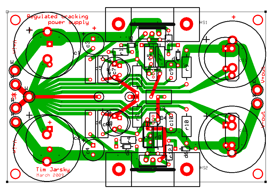
here is the most recent version of the pcb for PS. it includes the LM329B's for the high stability version. I have also included protection diodes from adjust bypass caps as well as output caps. This makes the board fully compatible with lM317/337s.
i have also found that the panasonic FM series caps have very low esr and may serve to significantly flatten the output impedance curve of the supply. There is the possibility that this combo could cause resonance but i will measure to ensure this is not the case.
lastly, i placed multiple lead spacings in 3 capacitor positions on the PCB. The one i am most interested in experimenting with is adjust pin bypass cap.
bypass capacitor testing
I have configured my board to allow for bypass capacitors (caps paralleling other caps) in several positions in my circuit board design.
The reason for doing this is that the bypass cap can bypass at frequencies where the higher value cap is inductive. This should reduce the noise level compared to the unbypassed configuration.
The risk is that the two caps impedance curves cross at steep parts of their curves and resonate.
To select the ideal cap combination's for my power supply so that i can avoid resonance, i needed a way to test for the effect of the bypass cap. Today i did a dry run of my testing procedure that i will use when the boards and parts do finally arrive (have not ordered yet, still tweaking design).
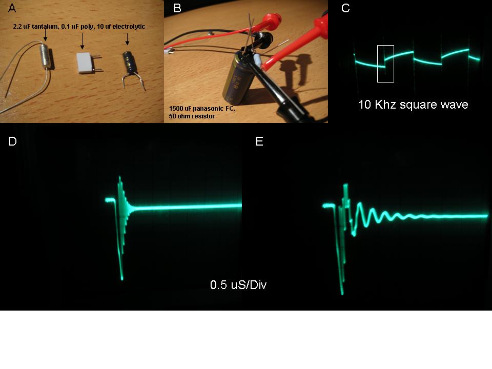
Methods: Used a function generator to generate a 10 khz, 5V square wave. Used 50 ohm BNC cable terminated with a 50ohm resistor. Had 10Volts DC on the output of the generator to put the caps under test near their operational voltage. Ran the output of the function generator across a 1500 uF panasonic FC cap and then tried hooking up different bypass capacitors (see A). For more info see: http://emcesd.com/tt020100.htm
In the attached figure you can see in A. The bypass caps i tried. B The test set-up without any bypass caps in the circuit. C the 10 khz square wave. The white square indicates the region magnified in D and E. D. Is the oscillation that the 1500uF cap produces on its own due to its parasitic inductance. E. Is the 1500 uF cap bypassed with the 0.1 uF poly cap. It greatly increased the oscillation. My scope is only 20Mhz so i am likely not seeing some of the "dammage" the poly bypass cap is causing. In D and E the voltage scale is 10 mV per division.
Both the tantalum and the electrolytic damped the oscillation somewhat. This effect was difficult to capture in a photo so here are the links to a .mov file for each cap:
electrolytic
Tantalum
In each movie i am connecting and disconnecting the bypass cap several times.
here is the figure:
I have configured my board to allow for bypass capacitors (caps paralleling other caps) in several positions in my circuit board design.
The reason for doing this is that the bypass cap can bypass at frequencies where the higher value cap is inductive. This should reduce the noise level compared to the unbypassed configuration.
The risk is that the two caps impedance curves cross at steep parts of their curves and resonate.
To select the ideal cap combination's for my power supply so that i can avoid resonance, i needed a way to test for the effect of the bypass cap. Today i did a dry run of my testing procedure that i will use when the boards and parts do finally arrive (have not ordered yet, still tweaking design).
Methods: Used a function generator to generate a 10 khz, 5V square wave. Used 50 ohm BNC cable terminated with a 50ohm resistor. Had 10Volts DC on the output of the generator to put the caps under test near their operational voltage. Ran the output of the function generator across a 1500 uF panasonic FC cap and then tried hooking up different bypass capacitors (see A). For more info see: http://emcesd.com/tt020100.htm
In the attached figure you can see in A. The bypass caps i tried. B The test set-up without any bypass caps in the circuit. C the 10 khz square wave. The white square indicates the region magnified in D and E. D. Is the oscillation that the 1500uF cap produces on its own due to its parasitic inductance. E. Is the 1500 uF cap bypassed with the 0.1 uF poly cap. It greatly increased the oscillation. My scope is only 20Mhz so i am likely not seeing some of the "dammage" the poly bypass cap is causing. In D and E the voltage scale is 10 mV per division.
Both the tantalum and the electrolytic damped the oscillation somewhat. This effect was difficult to capture in a photo so here are the links to a .mov file for each cap:
electrolytic
Tantalum
In each movie i am connecting and disconnecting the bypass cap several times.
here is the figure:
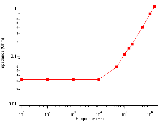
Zout measurement
I think i now have a reasonable test set up to measure the output impedance (Zout) of the power supply.
using a function generator and an oscilloscope i was able to measure Zout from 1000hz to 2Mhz.
The lowest measured Zout was 0.2 ohm. I believe this is as a result of taking measurements using the prototype board because if i take a resistance measurement between two relatively distant points on the board (5 inches apart) i measure 0.2 ohm. Hopefully the thick traces on my pcb will overcome this problem and lower Zout by an order of magnitude. Is this a reasonable hypothesis?
Noise levels will also limit the minimum Zout i can measure as i need to be able to resolve amplitudes of less that a mV. Right now i have about a mv of peak to peak noise. Time to build a mini faraday cage and maybe use my work oscilloscope.
One issue i noted was that above 10khz i started to get a small oscillation (approx 5 mV in amplitude). I assume this is as a result track inductance as changing caps did not seem to make a difference. As above, i hope that the use of the PCB resolves this issue.
The last remaining test i want to be able to do is to measure the transient response. I was hoping to be able to run a relay directly of the function generator and have the relay load and unload the power supply. Can someone recommend a relay that can run directly from a function generator and switch at fairly high frequencies?
i am looking forward to reporting the effects of cap selection on Zout, Transient response, and noise levels. I expect there might be some interesting tradeoffs.
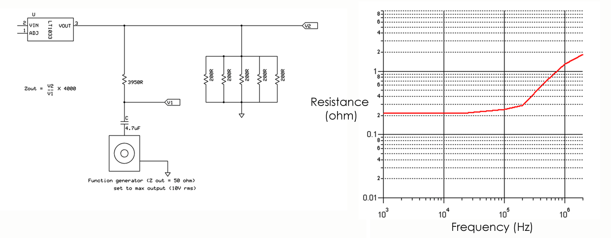
here is the schematic for measuring Zout as well as the Zout vs Frequency plot.
I think i now have a reasonable test set up to measure the output impedance (Zout) of the power supply.
using a function generator and an oscilloscope i was able to measure Zout from 1000hz to 2Mhz.
The lowest measured Zout was 0.2 ohm. I believe this is as a result of taking measurements using the prototype board because if i take a resistance measurement between two relatively distant points on the board (5 inches apart) i measure 0.2 ohm. Hopefully the thick traces on my pcb will overcome this problem and lower Zout by an order of magnitude. Is this a reasonable hypothesis?
Noise levels will also limit the minimum Zout i can measure as i need to be able to resolve amplitudes of less that a mV. Right now i have about a mv of peak to peak noise. Time to build a mini faraday cage and maybe use my work oscilloscope.
One issue i noted was that above 10khz i started to get a small oscillation (approx 5 mV in amplitude). I assume this is as a result track inductance as changing caps did not seem to make a difference. As above, i hope that the use of the PCB resolves this issue.
The last remaining test i want to be able to do is to measure the transient response. I was hoping to be able to run a relay directly of the function generator and have the relay load and unload the power supply. Can someone recommend a relay that can run directly from a function generator and switch at fairly high frequencies?
i am looking forward to reporting the effects of cap selection on Zout, Transient response, and noise levels. I expect there might be some interesting tradeoffs.
here is the schematic for measuring Zout as well as the Zout vs Frequency plot.
corrected movie links
the links showing the effect of the different bypass caps in post 27 are incorrect.
here are the correct links:
electrolytic
tantalum
the links showing the effect of the different bypass caps in post 27 are incorrect.
here are the correct links:
electrolytic
tantalum
Zout measurement update and other error corrections
1. i have been able to improve my Zout measurement technique and am beginning to approach the expected impedance (<0.01 ohm from 100 to 1000 Hz). I reduced the value or the resistors in the test circuit to 2000R and 20R. By doing this i am able to increase my signal to noise.
i will not be able to obtain a lower output impedance measurements on the prototype board because the noise floor is too high. I can't compensate for this by lowering the value of the function generator series resistor any further because this would also require increasing the load (reducing the resistance of the load resistors). On the prototype board i don't have room for a heat sink so the regulator can't handle much more than 400mA i currently test with before protection kicks in.
2. I am also making progress on testing the transient response. I've decided that a relay is the wrong approach because of switching time and bounce. Instead i plan to use an optocoupler to drive a transistor which will control the load.
3. It also looks like the oscillations i saw when testing bypass capacitors are likely the result of the test equipment. Here is what my friend at work said who repeated my test with a slightly different set up which he explains:
"I charged a cheaper Panasonic cap (‘M’ series, 85degC, 3300mF@35V) to about 18V, then shorted the ends of the leads together while measuring at the base of the leads, thinking that any series resistance added might hide ringing. There was almost no internal inductance suggested by this test, near perfect voltage drop. Interestingly, the single cap behaves like two caps in parallel: there is an immeasurably fast drop of about a quarter the voltage that occurs within a few nanoseconds, like a small cap with little internal resistance would do, followed by a pause or even rebound (This suggests inductance, with two time constants like the capacitance) and then a much slower drop occurring over a half millisecond, like a 3300mF cap with internal resistance of very roughly 0.1R. I think Panasonic designed these caps for this behavior. I’ll attach pictures I took at two time scales, both showing only the initial drop and rebound. It’s possible I’m measuring the properties of the weld formed when the leads are forced together – there is a distinct snap – rather than the cap properties. So, next I tried discharging through a 20R resistor, to be close to comparable to what you did. Perfect behavior, no visible ringing or deviation from an exponential curve at all, but of course discharge took over 100ms to mostly finish. Same thing with 50R, just a slower drop predicted by RC. Same results with rising edges, cramming the resistor lead onto the discharged cap after connecting the resistor to 18V. I think the caps are so near perfect that we would have to either send radio frequencies into them or design new equipment to reveal their shortcomings, for which I do have some starting ideas. I hold fast to my original belief that it is much more likely that the caps are revealing imperfections in the test set up than the other way around, but I’d love to be proven wrong."
and here is a scope pic of the results he obtained.
I should add that bypassing with a couple of caps we had on hand did not significantly alter the response shown above.
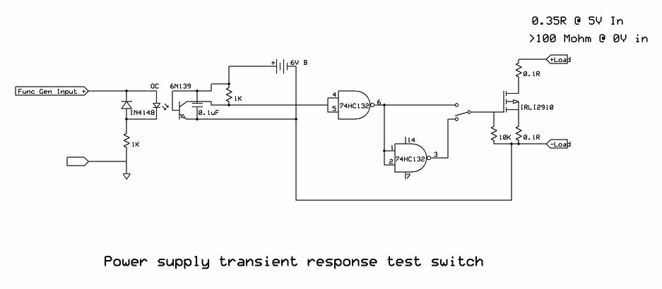
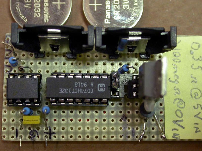
Load Switch prototype
In the previous post i mentioned that the oscillations i observed while testing caps with a function generator were likely the result of the test equipment and not the cap itself.
i also mentioned wanting to test the power supply transient response.
To do these task i wanted a switch that could be controlled from a function generator. The switch needed to have a very fast switching time as well as little to no bounce. Slow switching and/or bounce would likely obscure the transient response i want to observe.
To do this a coworker developed a load switch for me. It consists of a transistor used as the switch. The transistor is controlled with a schmidt trigger and these devices are isolated from ground with a optocoupler. The optocoupler receives input from a function generator.
I'll hopefully have some test results to report soon.
here is the schematic:
here is a pic of the prototype:
Hi Marce,
please feel free to ask as many questions as you like. i appreciate your interest.
i chose a star ground because i think it is the best way to ensure that there are no ground loops.
i think you are correct in pointing out that long narrow traces will add resistance. i have done my best to maximize the trace thickness given the space constraints.
i am still tweaking so i'll see if i can still find room to widen some of the narrowest traces and/or shift the star closer to the center of the board.
here are a couple of the references i based my decision on:
http://www.epanorama.net/documents/groundloop/in_circuit.html
http://www.national.com/an/AN/AN-1490.pdf
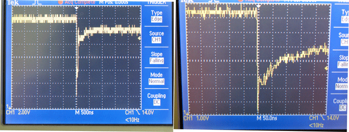
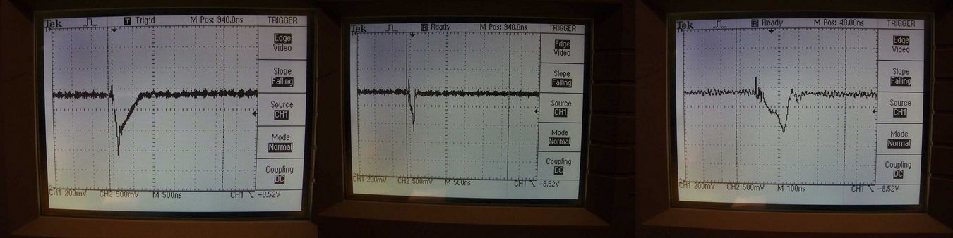
Transient response test update
Using my load switch i was able to successfully test the transient response of my prototype power supply.
I used a 0.33 amp load and looked at the effect of swapping output capacitors - 10uf and 1500uf (both panasonic FC).
Left scope pic - 10 uf (500 mv/div, 500 ns/div)
Middle scope pic - 1500 uf (500 mv/div, 500 ns/div)
Right scope pic - 1500 uf (500 mv/div, 100 ns/div)
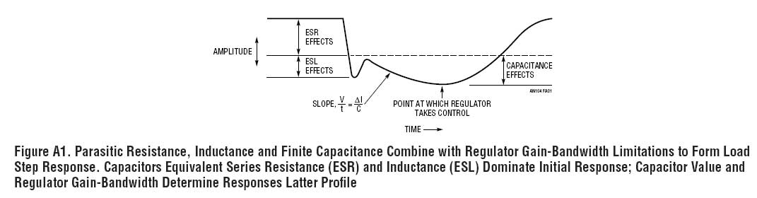
Below is a Figure from:
http://www.linear.com/pc/downloadDocument.do?navId=H0,C1,C1003,C1142,C1041,P1754,D17358
that explains the transient response profile. The 10uF cap transient response seems well matched to the representative profile, but, the the 1500uf does not.
Also, the duration of the transient response is consistent with those reported in the above article, but the amplitude is significantly greater. I don't have an explanation for for the difference in transient amplitude. Things may improve when i move from the prototype board to the circuit board. It could also be that i was not measuring directly from the output pin of the regulator. I expect that the test conditions were better optimized in the linear article.
Note** The load switch takes less than 20 ns to switch. I may try to improve the switching time with the use of a faster transistor.
Using my load switch i was able to successfully test the transient response of my prototype power supply.
I used a 0.33 amp load and looked at the effect of swapping output capacitors - 10uf and 1500uf (both panasonic FC).
Left scope pic - 10 uf (500 mv/div, 500 ns/div)
Middle scope pic - 1500 uf (500 mv/div, 500 ns/div)
Right scope pic - 1500 uf (500 mv/div, 100 ns/div)
Below is a Figure from:
http://www.linear.com/pc/downloadDocument.do?navId=H0,C1,C1003,C1142,C1041,P1754,D17358
that explains the transient response profile. The 10uF cap transient response seems well matched to the representative profile, but, the the 1500uf does not.
Also, the duration of the transient response is consistent with those reported in the above article, but the amplitude is significantly greater. I don't have an explanation for for the difference in transient amplitude. Things may improve when i move from the prototype board to the circuit board. It could also be that i was not measuring directly from the output pin of the regulator. I expect that the test conditions were better optimized in the linear article.
Note** The load switch takes less than 20 ns to switch. I may try to improve the switching time with the use of a faster transistor.
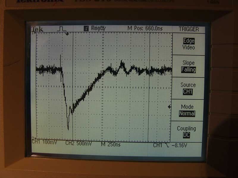
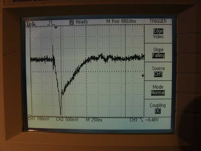
LT1033 vs LM337 transient response
today i compared the transient response of the LT1033 to the LM337.
i also tried 3 different output capacitors but the results were consistent across the different cap types so i am only showing scope pics with the 10uf panasonic FC output cap.
The transient response of the regulators was very similar. The peak voltage deflection of the LM337 was always a bit smaller than the LT1033 - about 10%. However the time to settle was longer with LM337 than the LT1033 - about 20%.
I did not look at the variability in transient response across regulators of the same type so i am not sure if these small differences will hold.
Take home message- LT1033 and LM337 have a very similar transient response.
here is the scope pic of the LM337 transient response to the same load as in previous post (note the wobble as the voltage returns to the set point):
here is a scope pic of the LT1033 transient response (note the relatively reduced amplitude wobble as the voltage returns to the set point)
Hi,
I've been studying you PCB layout and would like to comment if you dont mind.
The star grounding worrys me, it has its place in amps and some circuitry, but I think in a power supply it may cause more problems than its worth. PCB design is about controlling current loops, both in the actual signal trace and more importantly its return path (commonly called GND ). In a power supply there are certain elements that have to be closely related, the first major loop is the input - output caps GND connection, these need to be close together either by low resistance for linear supplys to low impedance for switch mode as this is the current loop through the regulator. The connection from the feed back resistors potential divider to the regulator must be as short as possible (these are quite often high impedance inputs and as it is the start point of the regulation noise or voltage drops are going to effect the output), and this is one area where a seperate GND track is recomended from the GND point of the divider to the load GND point, again interefence on this line effects the control voltage. As to the rest I would siggest a ground plane on the bottom of the board, it tends to solve more problems than it causes. We use LDO's and switch mode supplys extensively at work and always follow the basic rules above.
Another problem you might encounter during the manufacture of the PCB is some of the acute angles may cause acid traps, this may cause over etching at theses junctions.
This link to National Semi is quite informative
http://www.national.com/appinfo/power/files/f4.pdf
These of course are my own opinions, I look forward to further discourse.
Thanks
Marc
I've been studying you PCB layout and would like to comment if you dont mind.
The star grounding worrys me, it has its place in amps and some circuitry, but I think in a power supply it may cause more problems than its worth. PCB design is about controlling current loops, both in the actual signal trace and more importantly its return path (commonly called GND
). In a power supply there are certain elements that have to be closely related, the first major loop is the input - output caps GND connection, these need to be close together either by low resistance for linear supplys to low impedance for switch mode as this is the current loop through the regulator. The connection from the feed back resistors potential divider to the regulator must be as short as possible (these are quite often high impedance inputs and as it is the start point of the regulation noise or voltage drops are going to effect the output), and this is one area where a seperate GND track is recomended from the GND point of the divider to the load GND point, again interefence on this line effects the control voltage. As to the rest I would siggest a ground plane on the bottom of the board, it tends to solve more problems than it causes. We use LDO's and switch mode supplys extensively at work and always follow the basic rules above.Another problem you might encounter during the manufacture of the PCB is some of the acute angles may cause acid traps, this may cause over etching at theses junctions.
This link to National Semi is quite informative
http://www.national.com/appinfo/power/files/f4.pdf
These of course are my own opinions, I look forward to further discourse.
Thanks
Marc
Hi Marce,
thanks for your comments. This is my first top to bottom electronics project as well as my first pcb design so i am looking for as much input as possible.
My response has taken so long because i have been doing a lot of reading on this topic, here on diyaudio, and elsewhere. Despite this effort i am still a bit confused, perhaps more now than before, about what is the best approach. In an effort to extract more info from you i am going to continue to advocate for the star ground and i look forward to responses.
I have responded item by item below.
marce said:Hi,
PCB design is about controlling current loops, both in the actual signal trace and more importantly its return path (commonly called GND
To better understand the implications of this comment can you tell me what the current loop in a bipolar supply looks like? How is it different from a single sided supply?
In a power supply there are certain elements that have to be closely related, the first major loop is the input - output caps GND connection, these need to be close together either by low resistance for linear supplys to low impedance for switch mode as this is the current loop through the regulator.
I totally agree that the input and output caps need to be well coupled. My question is, what trace width has the same effective resistance as a ground plane? I assume that at some point widening the trace will not greatly effect the resistance between the two points. Can i approach this resistance using separate traces?
I think that by moving the star inward and widening some traces i can really make the trace resistances very low. Right now the narrowest trace is 0.04"(~1mm). According to this calculator:
http://circuitcalculator.com/wordpress/2006/01/24/trace-resistance-calculator
I get about 0.01 ohm per inch. If i keep the trace less than 3 inches that gives me a total resistance of 0.03 ohms. Is this considered significant resistance for an estimated output current of less than 300 mA?
The connection from the feed back resistors potential divider to the regulator must be as short as possible (these are quite often high impedance inputs and as it is the start point of the regulation noise or voltage drops are going to effect the output), and this is one area where a seperate GND track is recomended from the GND point of the divider to the load GND point, again interefence on this line effects the control voltage.
To address this issue i placed the first resistor (two resistors in this circuit) in the voltage divider as close as possible to the output pin and ran the trace in the most direct route possible back to the adjust pin. I could make this loop shorter if i used surface mount parts but for the sake of simplicity i am avoiding them.
Just to make sure we are on the same page, did you see that i have the adjust pin grounds coming together, but they are not presently hooked to anything else. My plan was to connect a wire from where they come together to the site of max load? This is essentially what is recommended in the data sheet as well as the reading you posted.
Do you think i should keep the adjust grounds separate and run two wires to the site of max load?
I also left the option, with the use of a jumper, to hook the adjust pin grounds directly to the star ground.
As to the rest I would siggest a ground plane on the bottom of the board, it tends to solve more problems than it causes. We use LDO's and switch mode supplys extensively at work and always follow the basic rules above.
Some here on diy audio recommend a star ground with a ground plane.
see here:
http://www.diyaudio.com/forums/showthread.php?postid=887542#post887542
What do you think about this?
Another problem you might encounter during the manufacture of the PCB is some of the acute angles may cause acid traps, this may cause over etching at theses junctions.
This was something i was totally unaware of. Is this a concern for all forms of pcb manufacturing?
This link to National Semi is quite informative
http://www.national.com/appinfo/power/files/f4.pdf
These of course are my own opinions, I look forward to further discourse.
Thanks
Marc
This was a great read. I finally have a handle on why they need to drop the gain as frequency increases. thanks so much.
Tim
regulator variability
Tonight i compared the transient response variability of the LT1033 and the LM337
LT1033 = 281 +/- 1.09 mV, n=10
LM337 = 281 +/- 2.67 mV, n=6
i'd call that an identical response, but the lm337 is more variable.
this variability was also reflected in Vreg. i frequently had to adjust the vertical position on the scope with each lm337 to keep the transient response on screen. I only had to do this only once with the LT1033.
Hi Okapi,
when I refer to current loops on PCB's, i am refering to the fact that any change to any signal be it analogue or digital has a equal and opposite effect in the return path, usually the GND return. The supply for this change comes ultimately from the power supply via reservoir and decoupling capacitors. So there is a multitude of current paths within a circuit. This is why in analogue amplifier circuits sperate GND returns are used, though theswe can be simplified into high current outputs, and low level signals. On a power supply though things are a bit different in that not only will the track resistance come into play but also its impedance. The impedance in tracks are what causes trouble as any change in current is going to be opposed by this inductance. An example of this inductive coupling in the path from the output caps to input caps on your PCB, the GND point of both these capacitors should be at the same voltage at all times, if you had a large transient on your output, the imediate current would be supplied via the output capactitors, this current is going to have to travel down a relatively thin, inductive track, if this causes a volage change then the amp is going try to compensate, this could cause bad regulation or oscillation.
What we do is colour the main current paths on the power supply schematic nad the these same paths can be drawn on the PCB. The aim is to determine the best grounding scheme for a paticular PSU topogrophy.
I will dig out some of my information as it is not that easy to explain in single post and there is a load of information about. We us numerous SMPS and LDO PSU's on our boards and recently worked with National Semi on our layouts to get the optimum performance wilst minimising EMC problems. Once you start visulising where the current loops are in a circuit it becomes clearer, and you can determine the best GND layout. Generaly star ground these days consist of a GND plane with strategic cuts in the copper to control current flow, this give the benefit of a low impedance plane, with the current control of starring.
As said I'll dig more info out, as its a large topic, I've been at it for 25 years and still learning.
The main differences between a GND plane and tracks are low impedance, signals can find the best return, be it low resistive reactance for low frequency to lpath of least inductance for higher frequency signals, plent of copper for current flow.
I would experiment with running the wires to the point of max load, a lot of data sheets assume quite often the point of load and power supply are quite close, if it was a commercial wstand alone supply, this point would be the output GND connector, and this probably isn't a bad starting point.
I put some more thoughts together later.
Marc
- Status
- This old topic is closed. If you want to reopen this topic, contact a moderator using the "Report Post" button.
- Home
- Amplifiers
- Power Supplies
- LT Dual Tracking 3A Regulated Power Supply 1.25V to 20V