Hi!
H have built a half bridge SMPS, wich uses a gate driver transformer, to drive the MOSFETs. The SMPS is working, the efficiency is not so bad at (relative) low loads.
The problem is (if it is really a problem, and not a measurement error), that the Gate-Source waveform looks like this:
http://sziget.mine.nu/~danko/aramkor/dscn1463.jpg
I connected the 'scope directly to the low-side MOSFET's pins.
At the circled parts, I think the MOSFET is turning on. The Gate-driver IC was TPS2811 (1.5A peak current), and when I changed to MC34151 (1.5A peak current), the left circled part "disappeared", but the right part was the same. Changing the IC to MC34151 improved the efficiency about 5-7%.
Oh, another important thing: The scematic:
http://sziget.mine.nu/~danko/aramkor/gkrellShoot_04-30-07_202558.png
The component values are not "top secret", I just turned them off, not to make the picture too "messy".
So, what do you think, SMPS gurus, why is there an undershot? Is that REALLY an undershot, or I just measure something wrong?
See this link and go to Page3 look at the gate drive transformer...
http://www.qscaudio.com/support/library/schems/Discontinued/PowerLight Series/PL1.0.pdf
http://www.qscaudio.com/support/library/schems/Discontinued/PowerLight Series/PL1.0.pdf
Those spikes in red circles are due to transformer leakage inductance and due to the own voltage drop of the driver IC, that usually results in a 2V dead band between sourcing and sinking current.
I think that the best solution is to use turn-off buffer transistors after the transformer, directly at the gates, to prevent the turn-off gate current from flowing through the windings (see other threads). Also, you should consider a driver IC with a MOS output stage, like IR4427, that does not exhibit voltage dead bands unlike ICs with bipolar output stages. Schottky diodes from the outputs to the rails may help with bipolar driver ICs when driving gate transformers, though.
Concerning the coupling capacitor, its purpose is to prevent gate transformer saturation (and smoke) in case of slightly asymmetric drive. You should rather leave it in the circuit

Hi,
I am also having trouble with gate trafo, but unlike Danko's mine doesent work. I'm using SG3525, min DT. Full-bridge configuration.
That's how the signal looks on gates, without any input voltave.
http://i206.photobucket.com/albums/bb166/BennyB1/gatedrivesignal.jpg
But when I applyed 30V the lower fets started to warm up.
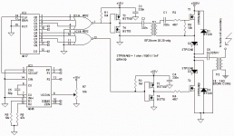
And here is the schematic I'm using.
http://i206.photobucket.com/albums/bb166/BennyB1/gatedrivesch.jpg
Note: there are 4 sec, I just didn't know how to do it
Edit: ups, D15 is a ZD15V.
I am also having trouble with gate trafo, but unlike Danko's mine doesent work. I'm using SG3525, min DT. Full-bridge configuration.
That's how the signal looks on gates, without any input voltave.
http://i206.photobucket.com/albums/bb166/BennyB1/gatedrivesignal.jpg
But when I applyed 30V the lower fets started to warm up.
And here is the schematic I'm using.
http://i206.photobucket.com/albums/bb166/BennyB1/gatedrivesch.jpg
Note: there are 4 sec, I just didn't know how to do it
Edit: ups, D15 is a ZD15V.
Can you give some more details such as power levels, input voltage, output voltage, and part numbers of components.
Minimizing leakage inductance in the drive xfmr is important. A drive capacitor as mentioned is important and also how is the layout? Were those drive signals taken at just bias or a 10kw load?
Can you try to put a local pull down transistor right on the FET? If you have a long drive run this will eliminate the discharge path.
Hi,
I whan't it to be 600W for now (hopefuly more). I tested it at 30V input, but like i said, the lower fets start to heat up).
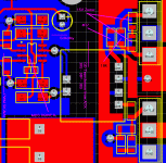
This is how the pcb for gate drive looks. The bufer on the primary side of the trafo is on the protoboard.
http://i206.photobucket.com/albums/bb166/BennyB1/PCB.jpg
The signals are on gates of two fets.
Nejc
I whan't it to be 600W for now (hopefuly more). I tested it at 30V input, but like i said, the lower fets start to heat up).
This is how the pcb for gate drive looks. The bufer on the primary side of the trafo is on the protoboard.
http://i206.photobucket.com/albums/bb166/BennyB1/PCB.jpg
The signals are on gates of two fets.
Nejc
Today I had time to experiment with my SMPS. I tried to load both the secondary and the primary winding with a resistor, but there was no improvement on the Gate signal.
I'm going to rewind the gate-driver transformer, maybe I can achieve lower leakage inductance.
Thanks for all Your advices!
I'm going to rewind the gate-driver transformer, maybe I can achieve lower leakage inductance.
Thanks for all Your advices!
In order to get "perfect" waveform, you need gate driver IC, such as MC34152.
I do this on my 750W half bridge AC/DC converter with Fsw 100khz, so the SG3524 osc 200khz.
The GDT is EE14, comes from ATX PSU, I heat the core to 400C with hot air solder for 2 minute, then GENTLY (it easy to crack) pull it out from the bobbin. Wound the secondary high side first (30T), the primary (30T), and the last low side secondary, in opposite direction (30T). All use 0.16mm(diameter) wire
You may want to read slup169.pdf from TI. There is alot of example about driving mosfet.
Anyway, anybody know how to do feedback with optocoupler?
Attachments
darw82 said:Anyway, anybody know how to do feedback with optocoupler?
Use a TL431 or even a zener with an opto
See figure 1 www.venable.biz/tp-17.pdf
And also figure 3 and 4 www.powerint.com/PDFFiles/techpapers/iic_011399.pdf
- Status
- This old topic is closed. If you want to reopen this topic, contact a moderator using the "Report Post" button.
- Home
- Amplifiers
- Power Supplies
- MOSFET driving with transformer