Except for clock distribution jitter issues. Even so that's unlikely to be significant (except in incompetent designs). Its more a measurement of Integral Nonlinearity and Differential Nonlinearity in the DAC and ADC. Also interesting would be the noise or randomness of the errors.
Hi, yes, sounds logical to me as well, the dac and adc are using same mclk and are probably triggered by same lrclk. but please look at that, just done few minutes ago
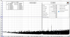
this is 2 RTA made with REW. first is EMU0404 in simple loopback. second is focusrite scarlett 6i6 2nd gen.
the jitter around the 1khz can be represented by the difference between the noise floor of the FFT and the point at say 999hz.
for the EMU it is 16db and for the 6i6 it is around 30 as you can see on the zoom...
so yes jitter should be represented here and fft should be very straight, but isn't.
for thoughts
Attachments
It can either be:
1- Clock distribution jitter (ie, DAC clock and ADC clock both pick up different amounts of noise). This can also happen if noise crosstalks into the clock traces, or DAC/ADC use two clock buffers with noisy power supplies, or noise on DAC/ADC digital power supplies, or clocks are routed through a FPGA, etc.
2- Noise on DAC or ADC voltage reference. Since the reference is a ... reference ... then DAC output voltage is the sample value multiplied by this reference voltage. Likewise ADC digital output value is analog voltage divided by its voltage reference. Noise (random, or fixed frequency) on the reference will cause a graph which looks exactly like jitter.
The way to know which is which is to measure it as 2 different frequencies, like 10k and 40k.
Jitter influence is proportional to signal slew rate, therefore frequency. If it is jitter, then the skirts will go up and down. Skirts at 40k will be 4x higher (12dB) than at 10k. And skirts at 10k will be 20dB higher than at 1k.
Noise on voltage reference is not affected by frequency. Skirts will be identical wether the test frequency is 1k, 10k or 40k.
For example, a buddy had spikes 50 Hz on each side of the test frequency, which were caused by 50Hz ripple on the reference voltage.
So if you post measurements at 1k and 10k (or higher) then we'll know !
Note that it's all pretty low here... -130dB... not that bad eh !
Interesting threat. I use E-MU-0202 for measurements. As long as no scope with its wide bandwidth is involved, loop measurements look fine to me.
If you replace DC-signal by a very low frequency of say 10Hz low distortion sine wave, you can observe level dependent noise possibly with you ears by reproducing the sound feeding some tweeter (piezo) speakers. At least this worked for me when investigating noise modulation of my first class-D attempts.
If you replace DC-signal by a very low frequency of say 10Hz low distortion sine wave, you can observe level dependent noise possibly with you ears by reproducing the sound feeding some tweeter (piezo) speakers. At least this worked for me when investigating noise modulation of my first class-D attempts.
Hi
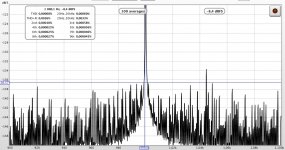
I ve been testing Jitter at 250hz, 1k and 4k on the Scarlett 6i6 and EMU0404
but then to interpret the results, I thought it would be better to use the phase noise sms jitter by applying the method and algorithm described in the following file:
https://www.advantest.com/documents/11348/1c6c5760-99f9-4b2e-b197-9ad2ae9e499c
so I ve done 6 RTA (64kFFT with 32 average) and then I used the save button to put them in the Measures and then file / export as text.
Then each file was imported in EXCELL and I ve kept only lines from fundamental +/- 10%
then I ve put some formula according to the paper above.
I get the following results:
Scarlett
250hz : 2158ps (-173dbc/Vhz)
1khz : 654ps (-184dbc/Vhz)
4khz : 234ps (-193dbc/Vhz)
EMU
250hz : 1410ps (-177dbc/Vhz)
1khz : 487ps (-186dbc/Vhz)
4khz : 210ps (-194dbc/Vhz)
the xls file is here
https://drive.google.com/file/d/0B5D8h5jG85DidzlfaTJZZWRrOWs/view?usp=sharing
the original mdat (rew) with the 6 fft is here.
https://drive.google.com/file/d/0B5D8h5jG85DiUzc0UG1VaG40aFE/view?usp=sharing
not sure how to interpret that and if my calculation are good or bad. may be someone has time to interpret or check this and come to some good conclusion ?
at least the good learning for me is that RTA can be exported into excel and then bins can be crunched to figure out some informations")
cheers
I ve been testing Jitter at 250hz, 1k and 4k on the Scarlett 6i6 and EMU0404
but then to interpret the results, I thought it would be better to use the phase noise sms jitter by applying the method and algorithm described in the following file:
https://www.advantest.com/documents/11348/1c6c5760-99f9-4b2e-b197-9ad2ae9e499c
so I ve done 6 RTA (64kFFT with 32 average) and then I used the save button to put them in the Measures and then file / export as text.
Then each file was imported in EXCELL and I ve kept only lines from fundamental +/- 10%
then I ve put some formula according to the paper above.
I get the following results:
Scarlett
250hz : 2158ps (-173dbc/Vhz)
1khz : 654ps (-184dbc/Vhz)
4khz : 234ps (-193dbc/Vhz)
EMU
250hz : 1410ps (-177dbc/Vhz)
1khz : 487ps (-186dbc/Vhz)
4khz : 210ps (-194dbc/Vhz)
the xls file is here
https://drive.google.com/file/d/0B5D8h5jG85DidzlfaTJZZWRrOWs/view?usp=sharing
the original mdat (rew) with the 6 fft is here.
https://drive.google.com/file/d/0B5D8h5jG85DiUzc0UG1VaG40aFE/view?usp=sharing
not sure how to interpret that and if my calculation are good or bad. may be someone has time to interpret or check this and come to some good conclusion ?
at least the good learning for me is that RTA can be exported into excel and then bins can be crunched to figure out some informations
cheers
Last edited:
Yeah, but you gotta be sure it's jitter.
I explained it could be jitter OR noise on the reference voltages.
You can determine which is which by eyeballing the skirts on both sides of your peak at different frequencies.
Skirts go up as frequency goes up: suspect jitter.
No change as frequency goes up: suspect voltage reference noise.
I explained it could be jitter OR noise on the reference voltages.
You can determine which is which by eyeballing the skirts on both sides of your peak at different frequencies.
Skirts go up as frequency goes up: suspect jitter.
No change as frequency goes up: suspect voltage reference noise.
Hi peu feu, thank you for your feedback, I hope I m not jeopardizing the thread. I just try to understand if this story about noise variation can have something to do with jitter
yes I understood your point, but I m questioning how to effectively measure the skirts... the way I did in my first post by looking at the db difference between bottom of fft and a point at +/- 0.1% of fundamental doesn't seem to me being a good way as the jitter phase noise is better representing by integrating something from a frequency f1 to say f2.
thats why i ve tried to quantify the jitter with the method I ve posted as a link.
And then we can see this value decreasing with the frequency, with a trend of about 9db/octave. so its not doubling as you mentioned in case of clock related jitter.
but all of that depends on the way we compute this jitter at a given freq.
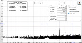
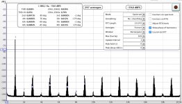
also, I was doing same kind of averaged FFT at -60db (ADC read with a 10db DAC signal and pot correction for -50db) and got this fancy figure which looks like a kind of j-test or result for a square signal
based on this , I ve used 16bits with dither and this has just reinforced the bin weight.
Can you or someone give feedback on how to interpret the ADC behavior based on this ?
thanks
yes I understood your point, but I m questioning how to effectively measure the skirts... the way I did in my first post by looking at the db difference between bottom of fft and a point at +/- 0.1% of fundamental doesn't seem to me being a good way as the jitter phase noise is better representing by integrating something from a frequency f1 to say f2.
thats why i ve tried to quantify the jitter with the method I ve posted as a link.
And then we can see this value decreasing with the frequency, with a trend of about 9db/octave. so its not doubling as you mentioned in case of clock related jitter.
but all of that depends on the way we compute this jitter at a given freq.
also, I was doing same kind of averaged FFT at -60db (ADC read with a 10db DAC signal and pot correction for -50db) and got this fancy figure which looks like a kind of j-test or result for a square signal
based on this , I ve used 16bits with dither and this has just reinforced the bin weight.
Can you or someone give feedback on how to interpret the ADC behavior based on this ?
thanks
Attachments
Last edited:
Your description of phase noise is correct when looking at the carrier. In this case there are several things making the display not directly applicable. I would suggest trying to duplicate John Atkinson's plots in Stereophile as a start.
Don't do this in a loopback since the common clock can mask a lot of issues.
The fundamental test frequency in the plot is important since the jitter sensitivity directly relates making comparisons difficult at best if you use a different frequency. Second using a frequency that is a submultiple of the sample rate removes some issues of DAC linearity etc.
Jitter will take two forms- deterministic jitter which will be distinct spectral lines that are symmetrical around the carrier and random jitter which is the noise floor rising.
You can start with a digital zero to see what the analog floor is. Then use a tone, usually per J dunn FS/4 (11.025 KHz for 44.1KHZ) You will see the sidebands and the floor will come up around the tone.
Look at the plots in Stereophile to get an idea of what to look for. He usually measures +/- 4 KHz from the fundamental and I think a translation is 192 KHz sampling + 64K points. Too little or too much will raise or lower the random noise sensitivity. The AP actually samples at a non-audio rate so some translation is needed. I'll try to confirm these numbers later today.
Measuring ADC jitter is more difficult. I used a precision crystal oscillator divided down to an audio frequency square wave and then took a high res FFT looking at the dispersion and sidebands around the fundamental as well as the noise. I did not learn a lot but it did seem that the ADC was not a limiter on measuring DAC jitter.
Hello
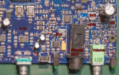
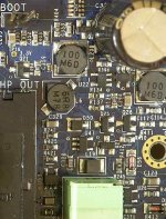
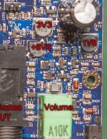
I don't want to do big modifications on my E-MU 0202, I just want to reduce the noise with simple modifications, any suggestions ?
First, on which pins at the 1V8 I should connect a capacitor on its output to reduce the 1MHz noise ?
And on which pins I should connect capacitor on the +3V3 , +6V4 and -6V4 output to reduce noise ?
Thank
Bye
Gaetan
Attachments
- Status
- This old topic is closed. If you want to reopen this topic, contact a moderator using the "Report Post" button.
- Home
- Source & Line
- PC Based
- Test bench: E-MU 0202 USB