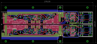
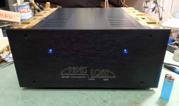
...... or - Look Ma, with no hands,Beast with thousand iterations!!

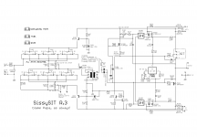
Logic demands that main schm is here, and all future edits, if and when needed
Few facts, for start, so when you ask, I can point you to this post:
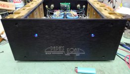
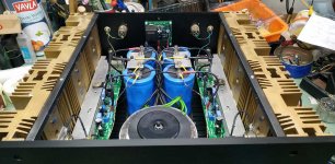
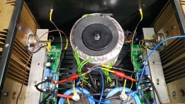
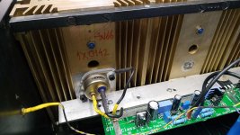
Rails - regular FW Format - in my case that is 300VA Donut per channel, 18+18Vac secondaries, two Graetz bridges per Donut
Iq - 1A7 to 1A8 ...... so dissipation per channel aroundish 80W
Autoformer - Cinemag CMOQ-4HPC
OS - generic ( means don't care which Factory) IRFP9140 and THF51S
Keratherm 86/82 pad for Mosfet, no-name silicon sheet for THF
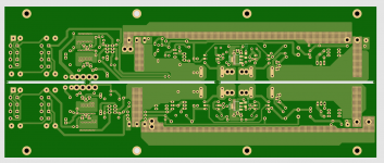
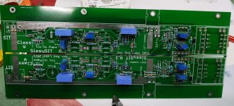
so, schm (as you can see, it is in fact simplified LuDEF ....... which is logical - this exactly lead me to LuDEF and few other Bstrd amps; stay tuned )
edit on 15.09.2021 - few general setting procedure tips and tricks:
-will not teach ya how to solder everything properly - as always -Assembly of Japanese Bicycle Require Great Peace of Mind
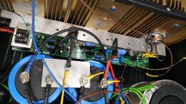
- one tip -SIT gate resistor - R126(226) - best to put shortie (0R) in pcb position, and put resistor itself heatshrinked to end of tiny wire and solder ditto to SIT gate
-prior to powering up, be sure that you have trimpots set properly:
P102 (P202) - irrelevant
P101 (P201) - set to max; confirm with ohmmeter across R104 - in vicinity of 28R
P103 (P203) -irrelevant
P104 (P204) - set to min ; confirm with ohmmeter - improvise where to put probes
- jumpers JP101/201 - open/not mounted
-as always - best to work with one channel connected to PSU at time; in fact - first step just one channel , in second step - you can freely leave powered/connected already set first channel
- one VMeter across output ( DC offset) , second VMeter across any of current sense 0R22 resistors; use mini-clips/probes
- no load on output, input shorted to GND
- power up thingie; observe DC offset - it will rise slowly and everything up to several volts is normal in this moment
observe VMeter across 0R22 resistor - it will be Dodo reading for some long time; after 60-90-120sec - if you don't see any substantial reading , start fiddling with P104 (P204), one turn at time; of course - you did remember where you rotate itr to set to min value, now rotate in counter direction; - don't ask me which - I don't care, I can't remember, simply because I'm always trusting in DMM, not in my memory how to orient damn trimpot to have screw in proper place ....... and my logic what needs to be decreased and what needs to be increased is always ooked, vs. overall consensus
allow 30sec or so between 1-turn steps, to observe when and how much mV you're getting across 0R22
goal is , , say for 1A8 of Iq - 1A8 * 0R11 = 198mV
keep fiddling to get mV creeping up, and once when you see steady rise for each turn, set da thingy to - say 160mV
once when you're there - fiddle with P103 to get as close to 0mV of output DC offset
that would be preliminary setting of OS, now to input buffer setting :
- power off , put mVmeter across R106(206) test pins ; put second mV meter on jumper pin marked "B" and GND
power on, fiddle with P101 to set 20mV across R106(206) ; done - fiddle with P102(202) to set as close to 0mV for buffer output offset ( second
mVmeter) ; when done - power off, close jumper
*************** connect second channel to PSU, repeat entire procedure******************
when done with both channels , power on , re-set Iq of both channels to have 1A8 (Square Law OS is crazy thing) somewhere in temp equilibrium, check output DC offset
slide of both Iq and DC offset - cold vs. hot - is really minimal, but I'm mentioning thermal equilibrium more thinking of importance of final temperature of heatsinks - observe, observe also temperature of outputs , that will give you info/confirmation how good and uniform is thermal interface between parts and heatsink
**************
when done, connect signal, speakers, flip da switch, and enjoy
don't forget Da Porn - no Porn, no Glory

Logic demands that main schm is here, and all future edits, if and when needed
Few facts, for start, so when you ask, I can point you to this post:
Rails - regular FW Format - in my case that is 300VA Donut per channel, 18+18Vac secondaries, two Graetz bridges per Donut
Iq - 1A7 to 1A8 ...... so dissipation per channel aroundish 80W
Autoformer - Cinemag CMOQ-4HPC
OS - generic ( means don't care which Factory) IRFP9140 and THF51S
Keratherm 86/82 pad for Mosfet, no-name silicon sheet for THF
so, schm (as you can see, it is in fact simplified LuDEF ....... which is logical - this exactly lead me to LuDEF and few other Bstrd amps; stay tuned
)edit on 15.09.2021 - few general setting procedure tips and tricks:
-will not teach ya how to solder everything properly - as always -Assembly of Japanese Bicycle Require Great Peace of Mind
- one tip -SIT gate resistor - R126(226) - best to put shortie (0R) in pcb position, and put resistor itself heatshrinked to end of tiny wire and solder ditto to SIT gate
-prior to powering up, be sure that you have trimpots set properly:
P102 (P202) - irrelevant
P101 (P201) - set to max; confirm with ohmmeter across R104 - in vicinity of 28R
P103 (P203) -irrelevant
P104 (P204) - set to min ; confirm with ohmmeter - improvise where to put probes
- jumpers JP101/201 - open/not mounted
-as always - best to work with one channel connected to PSU at time; in fact - first step just one channel , in second step - you can freely leave powered/connected already set first channel
- one VMeter across output ( DC offset) , second VMeter across any of current sense 0R22 resistors; use mini-clips/probes
- no load on output, input shorted to GND
- power up thingie; observe DC offset - it will rise slowly and everything up to several volts is normal in this moment
observe VMeter across 0R22 resistor - it will be Dodo reading for some long time; after 60-90-120sec - if you don't see any substantial reading , start fiddling with P104 (P204), one turn at time; of course - you did remember where you rotate itr to set to min value, now rotate in counter direction; - don't ask me which - I don't care, I can't remember, simply because I'm always trusting in DMM, not in my memory how to orient damn trimpot to have screw in proper place ....... and my logic what needs to be decreased and what needs to be increased is always ooked, vs. overall consensus
allow 30sec or so between 1-turn steps, to observe when and how much mV you're getting across 0R22
goal is , , say for 1A8 of Iq - 1A8 * 0R11 = 198mV
keep fiddling to get mV creeping up, and once when you see steady rise for each turn, set da thingy to - say 160mV
once when you're there - fiddle with P103 to get as close to 0mV of output DC offset
that would be preliminary setting of OS, now to input buffer setting :
- power off , put mVmeter across R106(206) test pins ; put second mV meter on jumper pin marked "B" and GND
power on, fiddle with P101 to set 20mV across R106(206) ; done - fiddle with P102(202) to set as close to 0mV for buffer output offset ( second
mVmeter) ; when done - power off, close jumper
*************** connect second channel to PSU, repeat entire procedure******************
when done with both channels , power on , re-set Iq of both channels to have 1A8 (Square Law OS is crazy thing) somewhere in temp equilibrium, check output DC offset
slide of both Iq and DC offset - cold vs. hot - is really minimal, but I'm mentioning thermal equilibrium more thinking of importance of final temperature of heatsinks - observe, observe also temperature of outputs , that will give you info/confirmation how good and uniform is thermal interface between parts and heatsink
**************
when done, connect signal, speakers, flip da switch, and enjoy
don't forget Da Porn - no Porn, no Glory
Attachments
Last edited:
Main reason/objective for this - third iteration of same amp is twofold :
- to enable use of any Ugs SIT ( so no more preferred range);
- to feed that little Devil in my head, saying all the time - "you didn't make it properly, you didn't make it properly..... "
I believe I succeeded in both")
To explain logic and problems, I think it's easiest to paste here few posts from LuDEF thread ( instead of putting links to them, I know many Greedy Boyz are if not lazy, they;re at least spoiled )
)
so, read this for fun .... if you already did, just skip down, unitil you see some porn posts
Biasing Mechanismus:
well, really nothing new under the Sun - meaning there is hardly anything specially new or unique that I put here
even if Papa really started us Greedy Boyz playing with Square Law OS arrangements, thing is old as Wheel, in fact
also - using rail series resistors, again Papa's bag of tricks ( for us) but again nothing especially new
neither source follower ( which is introduced here in front of upper output device) used as level shifter is anything new .....
thing is - it's hard to make anything absolutely unique, and wishing just that is right recipe to get yourself in not making anything at all ....... so , studying schematics from everywhere and one can just hope to get in situation to stand on Giant's shoulders
one day ...... one day ............
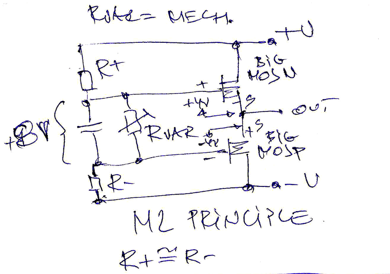
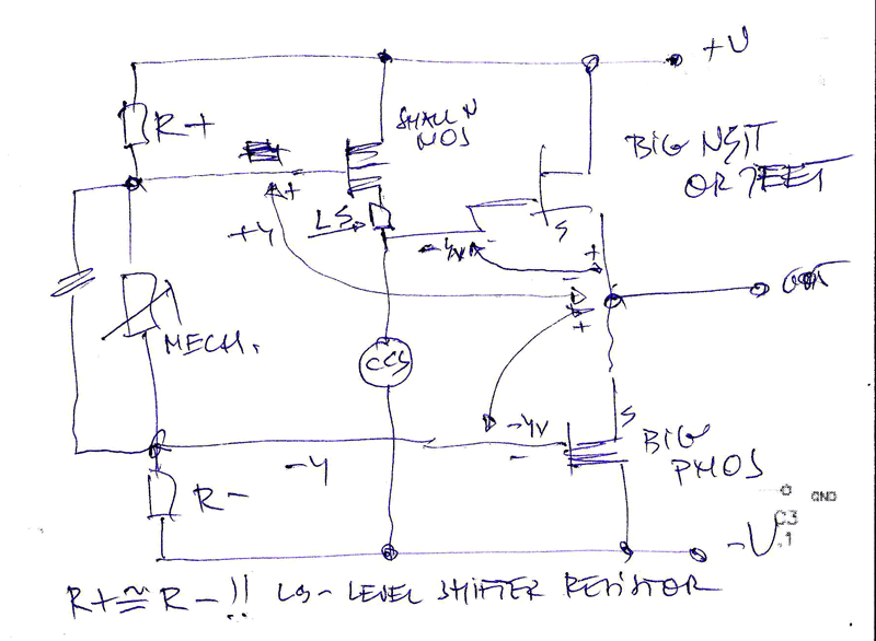
anyway - here is basic , lets call it , M2 biasing mechanismus;
simple as that:
we have R+ connected to upper part gate,
we have R- connected to lower part gate,
we have some variable impedance connected between gates; varying that impedance we are varying voltage sag across R+ and R- , thus positioning gates at appropriate voltage potential ( one vs. another) , thus setting how much Iq will pass trough output devices
call that variable impedance Rvar, further Mech. , shorted of mechanismus
cap between gates is there to eliminate AC to appear between gates - we don't want that ........ and also worth to mention - R+ and R- are sorta same in value , difference being just what we need to set output offset to 0 ( N gate and P gate voltages not exactly being identical)
- to enable use of any Ugs SIT ( so no more preferred range);
- to feed that little Devil in my head, saying all the time - "you didn't make it properly, you didn't make it properly..... "
I believe I succeeded in both
To explain logic and problems, I think it's easiest to paste here few posts from LuDEF thread ( instead of putting links to them, I know many Greedy Boyz are if not lazy, they;re at least spoiled
)so, read this for fun .... if you already did, just skip down, unitil you see some porn posts
Biasing Mechanismus:
well, really nothing new under the Sun - meaning there is hardly anything specially new or unique that I put here
even if Papa really started us Greedy Boyz playing with Square Law OS arrangements, thing is old as Wheel, in fact
also - using rail series resistors, again Papa's bag of tricks ( for us) but again nothing especially new
neither source follower ( which is introduced here in front of upper output device) used as level shifter is anything new .....
thing is - it's hard to make anything absolutely unique, and wishing just that is right recipe to get yourself in not making anything at all ....... so , studying schematics from everywhere and one can just hope to get in situation to stand on Giant's shoulders
one day ...... one day ............
anyway - here is basic , lets call it , M2 biasing mechanismus;
simple as that:
we have R+ connected to upper part gate,
we have R- connected to lower part gate,
we have some variable impedance connected between gates; varying that impedance we are varying voltage sag across R+ and R- , thus positioning gates at appropriate voltage potential ( one vs. another) , thus setting how much Iq will pass trough output devices
call that variable impedance Rvar, further Mech. , shorted of mechanismus
cap between gates is there to eliminate AC to appear between gates - we don't want that ........ and also worth to mention - R+ and R- are sorta same in value , difference being just what we need to set output offset to 0 ( N gate and P gate voltages not exactly being identical)
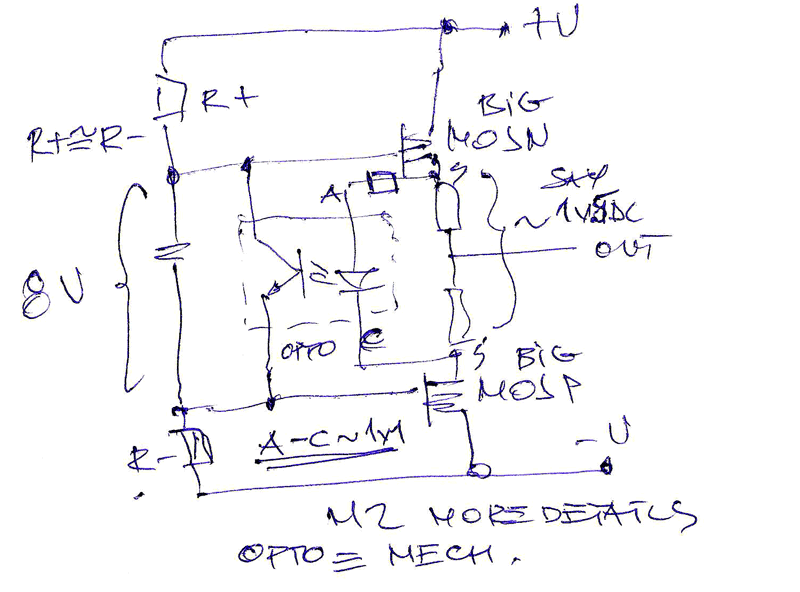
M2 in more details;
as said - it's relatively easy when we want to use source resistors as Iq reference points; I mean - easy when we got recipe from Mithrandir
also easy when we are using lower and upper output parts having so-so equal gate voltages, opposite side of output node, meaning +4V and -4V
optodiode connected across source resistors, series resistor to optodiode taking care that diode is not getting more than nominally 1V1 , at preferred Iq through source resistors
opto transisttor is now MECH. , governing current through R+ and R- , everything is Wine and Roses
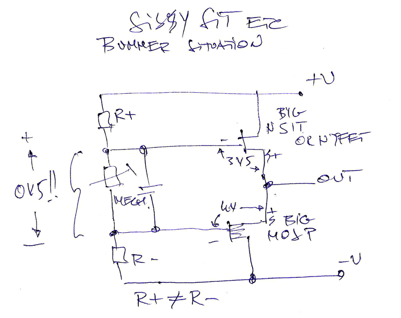
things are getting tricky when we want to use different part than Mosfet ( either up or down) , while using same biasing technique
say SissySIT (DEFiSIT) - Toking Bigun is different to N mosfet in that way that gate voltage is opposite in sign (differene between enhanced vs. depletion mode parts, +4V-ish vs. -3V-ish)
now voltage window between gates is no more twice 4v (+4V reaching down to -4V), now it is -3Vsomething reaching to -4V
we are happy campers if we have SIT with Ugs no greater in number than, say , 3V7 , so we have big enaough voltage window between gates, to squeeze optotransistor in
some P mosfets are having Ugs in range of -4V5, thus allowing as little broader batch of Tokins to be used, but that's just one more thing to take care with, endless parts picking .......
current through R+ and R- is, logically, one current; due to fact that gates are not symmetrical to output node, now R+ and R- can't be approx. same in value, resulting in few problems, of which most important one is that mains fluctuation resulting in sliding output DC offset , also parts TempCo playing game with Iq, then rails fluctuating down ( if not regged) etc.
Luckily , I succeeded more or less in set of compromises while making SissySIT , both first one and R.2
now, how to solve those issues ...... unequal Rail resistors , SIT parts with greater Ugs number ..... sometimes time is needed either to make space for new problems in thick skull, or just to have some leeway, then be able to step aside and look at problem from another point
level shifter part, that's it
small mosfet, so Ugs is sorta symmetric to big mosfet down Ugs, .... suddenly Rail resistors are sorta equal again, practically no gate currents to complicate things ( as is case with some not so well behaving Tokins)
principal schm down; ignore MECH. principle fro now
I think everything is clear, except note about LS resistor - its value is roughly SIT Ugs divided with current trough small Mosf/LS res./CCS ;say that you put value just being in ballpark; you can always go back and alter its value , to get wanted symmetry of lower and upper mosfet Ugs values
now, as all important is explained, time to mull about rail sense
I know for sure that Pa is using something in that manner already in PL products, but him being Pa - solving everything with resistors and zeners as level shifters
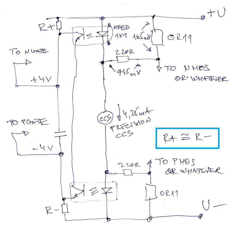
Mighty ZM , being chicken , I didn't up to recently even know that resistor can be described as CCS ( even if poor one), and I decided to use helper CCS ( see explanation) in form of ultramumbojumbo5$specialpart
in M2 case - wee see that optodiode is fed with voltage from source resistors, where we have voltage in abundance, even shaving it with series resistor
in SissySIT ( still damn good piece of work, if you ask Mighty Modesty Moi), I did use Hall chips ( tnx, Mighty Indra) ....... slope of voltage given at chip output is (2V5 to 5V)/(0 to 5A) ........ but effectively lower due to all summing and whatnot; didn't tried zeners as level shifters to decrease summing losses, but damn slope must be same , shifted with resistors or with anything else
working, but I maybe didn't knew that I can do better, but I obviously wished that I can do better, regarding Iq and offset stability in rail voltage/temp/time domains
so, if one choose to use ( minimal needed value of) rail resistors as current sense chain, even with 0R11 ( two of 0R22 in parallel) we have better effective voltage slope with current change ; numbers doesn't compute exactly, but from actual circuit, behavior is better than with Hall Chips
now ....... say that current is 1A5 , as in LuDEF
we have 165mV across 0R11 sense resistor......... ( I didn't want bigger value, sue me ...... later I got that voltage slope is enough with that value ) ..... but optoled needs nominally 1V1 to shine happily ............. so- there is a trick with helper CCS ( again, Pa using resistor there) , which is going to add some voltage to optoled - simple addition of 220R resistor and CCS pulling some current , we got additional 935mV
from there, when you gotta that optoled is shining happy, everything is just matter of more or less voltage through series 0R11
all that nicely transposed to opto in lower rail, so we now have rail resistors, each of them having own optotransistor to pull current trough, optotransistors are summed together
again, cap between two rail resistors, if using any of preceeding solutions with two mosfet gates ( one up, one down) we have symmetrical values of rail resistors, everything behaving nicely and polite and .......... almost boring
(M2 is same boring, regarding that)
so, what was left - put all these puzzle pieces on table and combine them
much greater problem is to choose which one of wast number of permutations is worthy of becoming an amp, than drawing any of them
if I forgot something , blame Pa
I know for sure that Pa is using something in that manner already in PL products, but him being Pa - solving everything with resistors and zeners as level shifters
Mighty ZM , being chicken , I didn't up to recently even know that resistor can be described as CCS ( even if poor one), and I decided to use helper CCS ( see explanation) in form of ultramumbojumbo5$specialpart
in M2 case - wee see that optodiode is fed with voltage from source resistors, where we have voltage in abundance, even shaving it with series resistor
in SissySIT ( still damn good piece of work, if you ask Mighty Modesty Moi), I did use Hall chips ( tnx, Mighty Indra) ....... slope of voltage given at chip output is (2V5 to 5V)/(0 to 5A) ........ but effectively lower due to all summing and whatnot; didn't tried zeners as level shifters to decrease summing losses, but damn slope must be same , shifted with resistors or with anything else
working, but I maybe didn't knew that I can do better, but I obviously wished that I can do better, regarding Iq and offset stability in rail voltage/temp/time domains
so, if one choose to use ( minimal needed value of) rail resistors as current sense chain, even with 0R11 ( two of 0R22 in parallel) we have better effective voltage slope with current change ; numbers doesn't compute exactly, but from actual circuit, behavior is better than with Hall Chips
now ....... say that current is 1A5 , as in LuDEF
we have 165mV across 0R11 sense resistor......... ( I didn't want bigger value, sue me ...... later I got that voltage slope is enough with that value ) ..... but optoled needs nominally 1V1 to shine happily ............. so- there is a trick with helper CCS ( again, Pa using resistor there) , which is going to add some voltage to optoled - simple addition of 220R resistor and CCS pulling some current , we got additional 935mV
from there, when you gotta that optoled is shining happy, everything is just matter of more or less voltage through series 0R11
all that nicely transposed to opto in lower rail, so we now have rail resistors, each of them having own optotransistor to pull current trough, optotransistors are summed together
again, cap between two rail resistors, if using any of preceeding solutions with two mosfet gates ( one up, one down) we have symmetrical values of rail resistors, everything behaving nicely and polite and .......... almost boring
(M2 is same boring, regarding that)
so, what was left - put all these puzzle pieces on table and combine them
much greater problem is to choose which one of wast number of permutations is worthy of becoming an amp, than drawing any of them
if I forgot something , blame Pa
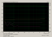
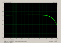
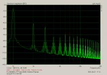
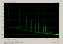
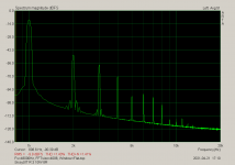
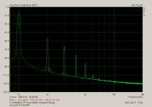
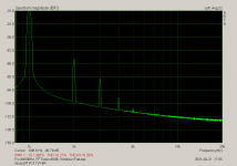
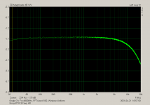
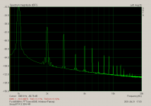
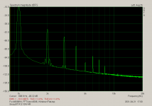
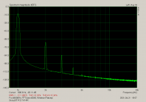
now, Measurements Porn
Iq 1A7
no significant difference between stone cold and Temp. equilibrium state
load 8R
Iq 1A7
no significant difference between stone cold and Temp. equilibrium state
load 8R
Attachments
-
 SissySIT R.3 THD vs. Freq. 8R.png47.3 KB · Views: 425
 -
 SissySIT R.3 Freq. 8R.png47.5 KB · Views: 486
 -
 SissySIT R.3 18W 8R.png46.9 KB · Views: 501
 -
 SissySIT R.3 15W 8R.png35.4 KB · Views: 469
 -
 SissySIT R.3 10W 8R.png33.9 KB · Views: 462
 -
 SissySIT R.3 5W 8R.png32.8 KB · Views: 585
 -
 SissySIT R.3 1W 8R.png31.2 KB · Views: 598
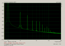
once more
Load 4R
Load 4R
Attachments
-
 SissySIT R.3 Freq. 4R.png48.2 KB · Views: 300
 -
 SissySIT R.3 20W 4R.png34.9 KB · Views: 296
 -
 SissySIT R.3 10W 4R.png33.6 KB · Views: 262
 -
 SissySIT R.3 5W 4R.png32.7 KB · Views: 310
 -
 SissySIT R.3 1W 4R.png31.6 KB · Views: 348
 -
 SissySIT R.3 15W 4R.png34 KB · Views: 266
 -
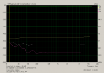 SissySIT R.3 THD vs. Freq. 4R.png47.3 KB · Views: 248


..........
..........
..........
Attachments
-
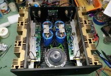 IMG_20210421_175949.jpg153.5 KB · Views: 898
 -
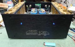 IMG_20210421_175940.jpg83.7 KB · Views: 753
 -
 IMG_20210421_175934.jpg82.8 KB · Views: 724
 -
 IMG_20210421_175926.jpg107.7 KB · Views: 717
 -
 IMG_20210421_171610.jpg119.2 KB · Views: 703
 -
 IMG_20210421_171604.jpg116.4 KB · Views: 1,114
 -
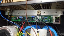 IMG_20210421_171601.jpg104.5 KB · Views: 1,154
 -
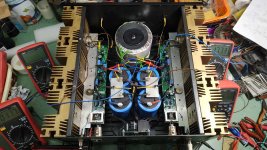 IMG_20210421_171554.jpg134.3 KB · Views: 1,178
 -
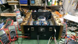 IMG_20210421_171548.jpg132.1 KB · Views: 1,206
 -
 IMG_20210403_210757.jpg104.4 KB · Views: 1,277
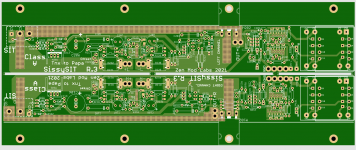
....matching of SITs - hard facts
as shown on two last pics in previous post - see specific part No. and Ugs of each - one is -3V66, second is -3V77 ( already established method - 24V@1A8)
so , they are so-so close by Ugs, and not matched in any way by curves ( don't have that thingie and certainly not going to have one)
find enclosed all measurements for both channels in one zip file
if you are curious enough to open it, you'll see that THD of both channels is very close ...... maybe it's just sheer luck I'm having ( that parts are close by curves) or DEF OS is really so magic and enigmatic concept..... in any case, I'm bedazzled with DEF concept - I mean in general - use of two dissimilar parts in arrangement usually reserved for max. possible complementary ones
Attachments
How it sounds.... will it drive F4?
Oh, yes - it sounds ... Spooky!
will it drive F4 - dunno, didn't tried
does it sound different to previous SissySIT iterations (both no-R and R.2) > no - there is no difference , simply because there is no other difference than made in biasing department
I was personally curious to establish is it going to be any difference, considering that SIT is now driven by source follower ....... and - nope, nada, zilch ........ SIT gate is enough benign and polite thingie to be driven, while small IRF source follower is enough benign and polite ..... I mean - benign and polite in context of generally so crude THD generator, which SissySIT certainly is
in my book, that's good enough Mimic of Papa's DEFiSIT
ZM Happy Camper, Omnilucky, avoided Public Disgrace once more
Level shifter resistor fine tune
schm, post #1 , resistor name is R115 and there is note beside
in later sketches - level shifting resistor, explained
goal is to have so so symetricall gate voltages of IRFP down and IRF up ....... (so DC offset behavior in Temp/time/mains voltage variations domains is predictable and minimally changing)
let's say that they are 4V nominally
logic is that source of IRF is approx at level of amp output
let's say that you know which Ugs is of SIT you're using ( even if you don't , easy to make adjustment later) ....... and let's say it is nice round figure of -3V
value of R115 needs to be adjusted in a way that we have voltage sag across exactly in value of SIT Ugs
and that's easy to compute - programmed current of Q103+T101 CCS is in range of 30mA, so for 3V voltage sag calculus is easy R=3V/30mA= 100R
in my case I did use 120R for both channels
in case that you're using unknown Ugs SIT - all you need after ballpark setting of Iq and DC Offset is to measure Ugs of M101 and M102, and fix** R115 to get them approx. same in absolute number
easypeasy
**it's cunning to solder there 1pin holders first then push preliminary/temporary resistor in; when final resistor is determined, just solder it in 1pin holders, for better sleep
would pack these 1pinners in kits, ZM Genius
Attachments

Last edited:
Congratulations for getting this ready. Does the R.3 work with THF-51N?
it'll work with any Tokin SIT you throw in
- Home
- Amplifiers
- Pass Labs
- SissySIT R.3