Thank you Biosonar for that info. It helps enormously.
I have thought that the J113/J175 version should have source resistors for power dissipation reduction. Now I will start a PCB for that configuration.
While we are talking about the J113, my datasheet shows gate at the left-most pin. The actual JFET has gate at the right-most pin. What is the deal with that?
For Idss, my J113 devices are all between 14mA and 28mA. I have tested hundreds. I bought a bag of 1000. Slowly working my way through them.
My J175 devices are between 20mA and 24mA. I have tested 100. More are on the way.
My assertion is that the combined Idss of each 1/2 of the buffer must match. The parallel buffer elements are all connected at the output.
So, there will be a PCB for un-degenerated FJETs like the J270 and 2SK304. That pcb is on the way to me. There will be a pcb for degenerated JFETs like the J113 and J175.
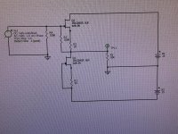
Here is another possibility for CCS mini-beast using the Toshiba 2Sk209 GB jfet. This design was suggested by Wayne from Pass Labs. Remove R4, R5 and add a gate resistor to the input:
I agree that a 2SK209/2SK208/2SK2145 massive B1 is a great idea. The trough-hole version is first on my list to build. The surface mount version for me will have to be assembled at a contract manufacturer.
Rochester has good candidates for through-hole JFETs. I have ordered some to evaluate. I will also build J113/J175 through-hole versions.
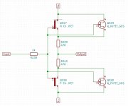
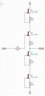
After new information from Biosonar, I have changed the basic cell. Here is the schematic.
I have added G-D-S transistors. The original transistors are D-G-S. Now the builder can choose D-G-S devices or G-D-S transistors. You can choose one of each.
The J113 is D-S-G and the J175 is D-G-S. These two can be used with this new board.
I have added G-D-S transistors. The original transistors are D-G-S. Now the builder can choose D-G-S devices or G-D-S transistors. You can choose one of each.
The J113 is D-S-G and the J175 is D-G-S. These two can be used with this new board.
Attachments
Last edited:
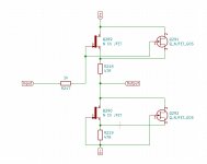
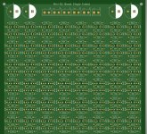
B1 Mini Beast
Both D-G-S and G-D-S pinouts are supported on this Mini B1 Beast
I am sorting the JFETs I have and have ordered additional types to characterize.
You can also use all P-JFETs if you reverse the power supply polarities. Aye, Keptin. Reverse the polarities.
Both D-G-S and G-D-S pinouts are supported on this Mini B1 Beast
I am sorting the JFETs I have and have ordered additional types to characterize.
You can also use all P-JFETs if you reverse the power supply polarities. Aye, Keptin. Reverse the polarities.
Attachments
Last edited:
Series B1 for extended voltage?
I have found a surplus JFET that is reasonably priced and has good gm and low noise. The limiting factor is that the device max voltage is 15v. If I want to use + / - 15v rails, is this a reasonable approach for the basic cell?
I have found a surplus JFET that is reasonably priced and has good gm and low noise. The limiting factor is that the device max voltage is 15v. If I want to use + / - 15v rails, is this a reasonable approach for the basic cell?
Attachments
well, not exactly
when you put more than one CCS in chain, there goes trouble
go here and download some reading material: Erno Borbely site , zip file - for benefit of DIY community - Zen Mod Blog
cascode them with bjts, shown in numerous Papa's thingies, same as in SissySIT etc.
when you put more than one CCS in chain, there goes trouble
go here and download some reading material: Erno Borbely site , zip file - for benefit of DIY community - Zen Mod Blog
cascode them with bjts, shown in numerous Papa's thingies, same as in SissySIT etc.
well, not exactly
when you put more than one CCS in chain, there goes trouble
go here and download some reading material: Erno Borbely site , zip file - for benefit of DIY community - Zen Mod Blog
cascode them with bjts, shown in numerous Papa's thingies, same as in SissySIT etc.
Ok Thanks. Will do.
well, not exactly
when you put more than one CCS in chain, there goes trouble
go here and download some reading material: Erno Borbely site , zip file - for benefit of DIY community - Zen Mod Blog
cascode them with bjts, shown in numerous Papa's thingies, same as in SissySIT etc.
I get a network error when I try to download your zip file.
take it from here: Dropbox - Borbely SITE.rar - Simplify your life
need to check what's the issue, with my Webhamster
need to check what's the issue, with my Webhamster
well, not exactly
when you put more than one CCS in chain, there goes trouble
go here and download some reading material: Erno Borbely site , zip file - for benefit of DIY community - Zen Mod Blog
cascode them with bjts, shown in numerous Papa's thingies, same as in SissySIT etc.
take it from here: Dropbox - Borbely SITE.rar - Simplify your life
need to check what's the issue, with my Webhamster
Got it. Thank you
")
I think you got a nod in Steve Guttenberg's latest interview with Papa.
BTW - Been following along even though a lot of this is far past my level of knowledge. Thanks for posting all the details, thoughts, and progress.
Thank you for the nudge to listen to the interview. Indeed the master mentioned this thread.
For sure, a multi-thousand JFET power amp will need to be surface mount. In the meantime, I am evaluating many JFETs. The test and debug boards have to be through-hole. These through-hole boards will be enough voltage and current to drive headphones and some flea-power speaker applications.
I may do a small-ish surface PCB as a trial run after the through-hole research is finished.
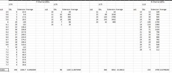
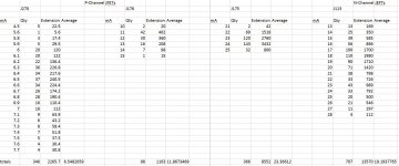
JFET Idss comparisons
Attached is a table of P JFETs compared against the J113.
There are no close matches.
My method will be to populate all of the lower Idss version, N or P and then populate enough of the other version, N or P to make the total Idss of each half close enough for very low output offset voltage.
This is for the complementary version. I want to be able to have a complementary version as well as a single ended version.
Attachments
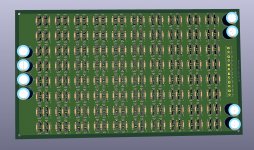
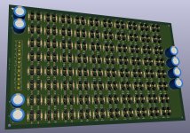
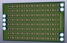
Single Ended Beast final layout
Updated silk screen. These final boards are universal for any pin-out of a JFET. You can have different pin-out top and bottom. D-G-S on top and G-D-S on bottom. Or vice versa.
You populate one JFET on the top of the cell and one on the bottom of the cell.
No need to identify P or N JFET. The board is populated with all N or all P.
Attachments
- Home
- Amplifiers
- Pass Labs
- Beast with 1000 JFETs redux?