
The LHS will work without the cap.
The RHS will not.
Correct ?
Patrick
Which cap are you referring to?
Let's be honest, any monkey can cobble a series of parts together, figuratively speaking.
I consider myself a cobbler, but most monkeys can't (figuratively speaking).
I consider myself a cobbler, but most monkeys can't (figuratively speaking).
Monkeys have even more common sense than I do!

 v=ir
v=irThe value for Rsen depends mostly on the bias current, optocoupler transfer ratio and LED parameters. The transconductance (gm) of the current source FET mostly affects value needed for Rmu for a given mu follower gain.lhquam, thank you for sharing those schematics.
Can I ask... you show a hockey puck, what's a good starting point for Rsen with IRFP in that config? (say... 1.6A, 39V V+ rail)
I am working on a presentation of the circuit equations for the mu follower and the Aleph circuits.
I have not actually built the circuit on the right using Rsen above the current source FET drain. In my build of the mu follower circuit, the voltage across RcsHI and Rmu is around 1.3V. At the 1.6A bias current, Rsen=RcsHI+Rmu would be about 1.3V/1.6A = 0.8125 Ohms.lhquam, thank you for sharing those schematics.
Can I ask... you show a hockey puck, what's a good starting point for Rsen with IRFP in that config? (say... 1.6A, 39V V+ rail)
Rsen=RcsHI+Rmu would be about 1.3V/1.6A = 0.8125 Ohms.
ahh I see now... the combined resistance of source sense is being used at the drain to maintain that operating point of the upper fet. Rmu is still Rmu. Thank you!
Aleph vs. mu-follower circuit equations
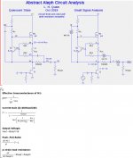
Shown below are abstractions of the mu-follower circuit of the FirstWatt SIT-2 and the Aleph Current Source as described in http://www.firstwatt.com/pdf/art_zv2.pdf. The mu-follower and aleph circuits have some commonalities and significant differences.
Commonalities:
Both circuits produce push-pull output from a single driver FET J1 and are characterized by their current gain and the load resistance seen by the drain J1.
Differences:
The aleph circuit equations are significantly more complicated than those of the mu-follower, the aleph having 7 parameters vs. 3 parameters of the mu-follower. The aleph circuit has the additional non-linear transistor Q1 inverter in the signal path to the modulated current source FET M1 vs. the direct (capacitor) coupled signal path from the J1 drain to the current-source FET gate.
The circuit equations of the abstract circuits were solved to obtain the current gain from the drain of the driver FET J1 to the output load Rload and to obtain the load resistance load line) seen by the J1. The complete systems of equations are available to those interested.
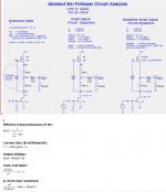
Attachments
- Status
- This old topic is closed. If you want to reopen this topic, contact a moderator using the "Report Post" button.
- Home
- Amplifiers
- Pass Labs
- Aleph current source vs mu stage?