Dear community
I just finished building my first F5 amp using the latest PCB's from the diyaudiostore. My setup is as follows:
- 240V input voltage
- 60W bulb in series with live wire
- soft start board from diyaudiostore (v3)
- 2x 18V toroid (300 VA)
- PSU v3 from the store including the diode section
- F5 PCB's from diyaudiostore (v3)
- with matched LSJ74/LSK170 JFET from the store
- with F5 transistor kit from the store
- speaker delay and dc protection board from the store
What I did to turn up so far:
- Connect mains to SS board: Works; relay switches very quickly (much less than half a second). Delay increases with a load.
- Connect toroid: Works; output is 2x 18 V.
- Connect PSU: Works; output is +/- 24 VDC (48VDC from V+ to V-). Very low discharging after power off (> 20 V after 5 minutes).
- Connect speaker delay board (from DC output of PSU, V+/GND): delay works; didn't test DC protection. Makes discharging of this PSU rail after switch off much faster (less than a minute).
- Connect first channel (input/output fully wired): works, meaning no smoke, soft start and speaker delay switch, bulb lights brightly for a short moment and dims significantly.
- Connect second channel: bulb lights brightly; speaker delay LED2 starts flashing and continues to light brightly but relays don't switch. Looks to me like a short circuit when adding the second channel F5 board.
- Same symptoms if I connect the possibly broken channel.
Now, I'm not a complete newbie (but still a newbie; built successfully a couple of chip amps and an Amp Camp Amp without issues). But with debugging the F5 board, I don't really know where to start.
- Are there any points where I can check a specific resistance?
- I did check for mixed up components and for FET orientation. All of them should be correct (and are identical to the other channel). Can I check the FET's without desoldiering them? My DMM does offer a diode test mode.
Thanks for any hints on how to start debugging this issue.
Daniel
- Connect first channel (input/output fully wired): works, meaning no smoke, soft start and speaker delay switch, bulb lights brightly for a short moment and dims significantly.
- Connect second channel: bulb lights brightly; speaker delay LED2 starts flashing and continues to light brightly but relays don't switch. Looks to me like a short circuit when adding the second channel F5 board.
Looks like you already have a working channel.
Use it for comparision to other (possibly shorted) channel?
Also, Is this tests done before or after bias&offset adjustments?
If it is made before; check potentiometers for second channel. If bias is high enough dim bulb will never goes dim. If it is too high or offset is not between tolerable value, dc protection may not allow relay to open output.
Sb.
Also, Is this tests done before or after bias&offset adjustments?
If it is made before; check potentiometers for second channel. If bias is high enough dim bulb will never goes dim. If it is too high or offset is not between tolerable value, dc protection may not allow relay to open output.
My test is before bias and offset adjustments. I thought the bulb test would make clear if there's an issue or not. Shall I proceed with the biasing with the bulb still in line with hot mains?
Daniel
My test is before bias and offset adjustments. I thought the bulb test would make clear if there's an issue or not. Shall I proceed with the biasing with the bulb still in line with hot mains?
Daniel
Proceed with the bias with 100w bulb. You'll see if you increase bias to 300-400mv, bulb begins to get bright. If you continue to increase, it will glow brighter. Leave it at %70 (if you aim for 1.3A, stop at 0.8-0.9A) and remove bulb and continue with the bias and offset adjustments. Bias adjustments need to be made step by step, if you try to make it quickly, you'll loose dc offset tracking.
Use three DMM.
I finally found some time to debug my setup. And there must be definitely some other issue than just the biasing. Here are some of my findings:
- While powered off, there's a resistance of 5 ohm between V+ and V- on the broken channel (indefinitely on the working channel).
- While powered on, the output voltage of the PSU is only 1.6 VDC (48 VDC with the working channel only).
- I double checked that all components and their orientation are identical for both channels. They are.
- I visually checked all soldier points and couldn't find any obvious issue.
Now, where shall I start so search for an issue? Any ideas what to look for without desoldiering?
Thanks,
Daniel
disconnect channel from PSU
-no continuity between mosfet's drains and heatsink
- no swapped mosfet places
-no swapped JFet places
-no swapped small bjt places
-check mosfets with diode test - there must not be any shorts ; if something is suspicious or in doubt - remove them from pcb and check with simple mosfet matching jig - or just replace them with new ones
- if JFets are suspicious - out and check with simple JFet matching jig
-if bjts suspicious - just replace them
-check action of trimpots also - rotate in one direction and measure across parallel resistors ; rotate all the way contra , measure
except input JFets , all other parts are peanut price , so chill
it applies both to work and theory - when you take piece by peace , it's easier to manage and/or grasp what you're doing ; do not rush and try to enjoy in building , that way everything is easier
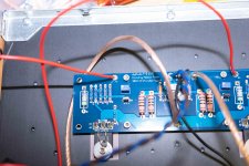
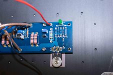
6L6, here you are. All pictures show the broken channel.
I actually tried some measurements following Zen Mod's advice. I did check for resistance between the heatsink and some components. First of all, I'm surprised that I do measure some 50 to 100 ohm of resistance almost everywhere (Mosfet pins, V+, V-) on both channels actually. But the main difference is that on the broken channel the source port of Q3 (P channel) shows almost no resistance to the heatsink (between 0.5 and 1 ohm). If I loosen the screw of Q3, resistance goes up to 100 ohm as well.
My expectation would be that there is no continuity between any component and the heatsink at all. Is this assumption wrong?
On the Mosfet's I installed one pad of Keraterm. Isn't this isolating enough?
Thanks,
Daniel
Attachments
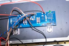
Thank you very much for all the hints. I've found the issue. It indeed turned out to be the thermistors touching the metal washers. I bent them further to touch the mosfet body instead. Couldn't find any further continuity between the heatsinks and any component.
Thanks,
Dani
Thanks,
Dani
Thank you very much for all the hints. I've found the issue. It indeed turned out to be the thermistors touching the metal washers. I bent them further to touch the mosfet body instead. Couldn't find any further continuity between the heatsinks and any component.
Thanks,
Dani
This has happened to me, and it burned up a trimpot.
The problem is that the thermistor's coating can be easily scratched...in my case it occurred when removing and reinstalling the PCBs several times. The thermistors would just get scratched when handling.
I put heatsink over them now. Yes, they won't be able to react as quickly but that is fine.
- Status
- This old topic is closed. If you want to reopen this topic, contact a moderator using the "Report Post" button.
- Home
- Amplifiers
- Pass Labs
- Debugging F5 - help needed