I am considering a standard aleph configuration using only two of the pucks in the attached datasheet. One on top and one on the bottom.
The goal would be to crank up the bias current to be in the 3A to 5A realm with 24V (or higher) rails and be able to operate into a very low impedance load. The puck is rated at 1040W dissipation at 25 deg C.
My guess is that the gate capacitance of the puck may be a problem.
At the moment, I am waiting on PCBs for the F4 Beast prototype and am considering some variants.
Suggestion/comments/jeers welcomed.
Attachments
Looking at the SOA curve, we see that it is a 90 watt part at 30V, and
that assumes 25 deg C case temperature. With a 30V rail and an ordinary
heat sink you will probably enjoy safe bias currents at an amp or so.
Not that you shouldn't go ahead and try it....
I get your point. The SOA is pasted here.
So, if the voltage is dialed back to 20V, then 7A is inside the DC SOA and 3A bias may be safe?
The other question is how small can the Aleph sense resistors be and the circuit still function as an Aleph?
Attachments
well , going for Aleph ..... you need that Vbe across upper source resistor
or , make it as fixed CCS in some other way , while obtaining proper modulation , so it still works as modulated CCS , with anything between 30 and 50% ( per wish) of sp called Aleph gain ( which is exactly percentage of contribution in output current)
or , make it as fixed CCS in some other way , while obtaining proper modulation , so it still works as modulated CCS , with anything between 30 and 50% ( per wish) of sp called Aleph gain ( which is exactly percentage of contribution in output current)
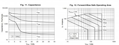
IXFN160N30T
From and SOA standpoint, this puck may be a better candidate for a high current single device Aleph. It is the IXFN160N30T. The datasheet does not show DC SOA but the DC SOA should be not very far inside the 1ms SOA curve. 5A at 30V should be safe for this device.
From and SOA standpoint, this puck may be a better candidate for a high current single device Aleph. It is the IXFN160N30T. The datasheet does not show DC SOA but the DC SOA should be not very far inside the 1ms SOA curve. 5A at 30V should be safe for this device.
Attachments
You'd better see Triode Transistor post #28 and #30.From and SOA standpoint,... does not show DC SOA ...
You'd better see Triode Transistor post #28 and #30.
I agree. If the datasheet does not show DC SAO, time to move on to the next part.
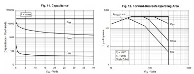
IXFN140N30P
This device looks promising. 700W DC Dissipation. 70A at 10V to 10A at 70V in a straight line.
In the 20V to 30V range, this part should have no problem being biased at 3A to 5A. 3A bias at 20V would be less than 10% of rated dissipation while 5A at 30V would be at 21% of rated dissipation. ....and.... it is not the most expensive puck on the ice rink.
Attachments
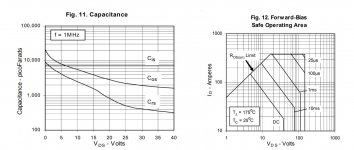
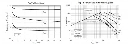
IXTN90NL25L2
Here is a third candidate. DC power dissipation 735W. Very similar SOA to the two good candidates above.
The interesting thing about this datasheet is that it shows SOA for Tc of 75 deg C. SOA decreases by almost 1/2 comparing 25C to 75C.
Here is a third candidate. DC power dissipation 735W. Very similar SOA to the two good candidates above.
The interesting thing about this datasheet is that it shows SOA for Tc of 75 deg C. SOA decreases by almost 1/2 comparing 25C to 75C.
Attachments
if SOA iz OK , then choose by capacitances
Agreed. I want to finish the survey of SOA candidates and then choose one. To your point, I have viewed more than one of the puck datasheet where the capacitance makes some crazy squiggles which caused me to move on to the next device. At the moment, I am only looking at devices in stock at Digikey.
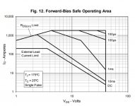
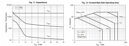
IXFN100N60P
Edit: part number IXFN100N50P
Here is the grand daddy of them all so far. 1040 watts DC dissipation.
At 30V Vds, the highest SOA current would calculate to 34.7 amps. That is about were the SOA curve is on the attached graph.
The capacitance curves are nicely behaved at 30V.
So far, this is the favorite for being able to bias it heavily.
Attachments
Don't be too sure.
Recommended reading:
https://ntrs.nasa.gov/archive/nasa/casi.ntrs.nasa.gov/20100014777.pdf
I like the quote at the top of page 9:
"the auto industry had found the problem in 1997. JPL then
reverted to “older parts,” and trusted the manufacturer to advertise
the problem; however, this never occurred"
Don't be too sure.
Recommended reading:
https://ntrs.nasa.gov/archive/nasa/casi.ntrs.nasa.gov/20100014777.pdf
I like the quote at the top of page 9:
"the auto industry had found the problem in 1997. JPL then
reverted to “older parts,” and trusted the manufacturer to advertise
the problem; however, this never occurred"
Wow. Thank you for the link and the nudge. I skimmed it quickly and it is not a skim kind of paper. It will take some time to digest.
Maybe I should rig up a test circuit with some lesser expensive MOSFETs to investigate the thermal runaway.
An article from Ixys Article_Linear_Power_MOSFETs_2007.pdf.... the thermal runaway.
That's a good one also, although the NASA paper and this one seem to
assign somewhat different causes to the problem.
In the Ixsys, they have solved it as follows:
"Every transistor cell is designed with a ballast resistor at the source
to limit its current."
In other words big die with many individual internal ballast resistors.
One of the draws to the big die transistors would be the ability to run
a large output stage without degeneration, making the most of the
square law character. Internal ballast resistors makes this less
attractive.
")
- Status
- This old topic is closed. If you want to reopen this topic, contact a moderator using the "Report Post" button.
- Home
- Amplifiers
- Pass Labs
- Hockey Puck Aleph