 Please don't start multiple threads for the same topic.
I have managed to draw up a schematic of my project amplifier and while it is most definately a Pass A40, it is not 100 true to the published information.
Your C4 compensation cap is huge electrolytic, the amp will work at DC only...
Maybe you would do better with 47 pf.
Where's the feedback resistor?
Input 2.2k resistor might want to be more like 1K.
That's all I saw in 30 seconds.
")
I have managed to draw up a schematic of my project amplifier and while it is most definately a Pass A40, it is not 100 true to the published information.
The amplifier uses two centre tapped transformers, one for each channel, it has a triac transistor in the power stage and a thermostatic switch, so I was hoping someone with the skill and knowledge would be willing to review the schematic and provide some feedback, maybe point out any potential design issues?
Thanks.
The type of transformer and the triac has nothing to do with the amplifier itself. Try to focus on one area, get that going, then look around to other victims ;-)
You have the original schematic from the article. That should be your reference.
BTW The speaker return should go to ground, not to the top of the R22.
Jan
Last edited:
Your C4 compensation cap is huge electrolytic, the amp will work at DC only...
Maybe you would do better with 47 pf.
Where's the feedback resistor?
Input 2.2k resistor might want to be more like 1K.
That's all I saw in 30 seconds.
My bad...... the schematic was wrong! Sorry.
C4 is actually 39pf 160v, not 470pf 25v as per the drawing.
Is the feedback resistor R13?
The input resistor is as spec at 2.2k, should I change it out to 1k?
Updated and correct schematic attached.
Thanks again.
Attachments
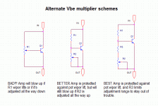
Here's a little tutorial on Vbe multiplier schemes. I fixed a Sony receiver that used the first scheme and blew expensive output transistors when the cheap carbon bias adjuster pot had a wiper lift. I lost respect for Sony product after that experience. I also replaced the faulty pot with a more reliable cermet multiturn unit.
Attachments
C4 is actually 39pf 160v, not 470pf 25v as per the drawing.
Is the feedback resistor R13?
It would be the first electrolytic 470 pF I will have seen.
R13 provides feedback about the output stage bias, but you are still
missing a resistor between the output and the Base of Q2. Something
like 2.2K @1 watt would do it.
Don't know if this is helpful or not, but just in case...
Thanks for the heads-up on this, I have checked it against my circuit board and the correction has already been made. Or it was never done incorrectly in the first place.
Thank you everyone....... it seems that the issue here was one of confusion and tiredness, along with a pinch of lack of knowledge!
I have just spent the last 4 hours going over the original schematic and checking it against my actual circuit board and I can confirm that almost everything is in order. However, there are one or two discrepancies between the schematic (fig 6, page 4) and the representative layout (fig 10, page 6):
1. On the schematic R4 is located on the negative side of C2, but on the layout is located on the positive side.
2. On the schematic D3 is located between the emmitter of Q7 and R13, but on the layout it is located after R13.
Can anyone confirm if these observations are correct and if they are of any consequence which is the correct layout???
On another note, regarding the the use of a 10k trimpot in place of R11 & R12, I have advised the following:
"R11+R12 should *NOT* be replaced by a trimpot as that prevents the bias limiting safety circuit (D3, R13) working properly if you turn the trimpot too far.
Instead R11 should be replaced by the trimpot, wired as a variable resistor, keeping R12 as specified on the schematic.
Provided you refit R12, the trimpot's dissipation will be negligible as there should never be more than 4V across the Vbe multiplier."
Would anyone with knowledge of the circuit agree with this?
Thanks for your patience!
Attachments
1. C2 and R4 are in series, so their order is irrelevant.
2. D3 and R13 are in series, so their order is irrelevant.
Did you make certain that the speaker return is not to the top of R22 but to ground, and that the feedback resistor is in place?
The bit above about the bias circuit is not specific to this circuit but a thoughtful way to make the bias circuit more fail-safe and should be followed, but is not required to get the amp working.
Jan
Last edited:
1. C2 and R4 are in series, so their order is irrelevant.
2. D3 and R13 are in series, so their order is irrelevant.
Did you make certain that the speaker return is not to the top of R22 but to ground, and that the feedback resistor is in place?
The bit above about the bias circuit is not specific to this circuit but a thoughtful way to make the bias circuit more fail-safe and should be followed, but is not required to get the amp working.
Jan
Thank you Jan, yes R13 is definately present. This was my first attempt at drawing a schematic and the onset of tiredness and confusion won over in the end!!
I have ordered new trimpots and will follow the guidance as suggested.
Evening all,
Today I got to the stage of powering on the amplifier....... nothing blew up!!
I switched the amp on, both power supplies at the same time, there is a very slight buzz from the transformers but you need to have your ear near to the amp to hear it fully. I assume this is normal.
Within around 5 minutes the heatsinks got very toasty.
The first test I did was measure the DC offset at the speaker posts. With my multimeter set at 200mv I got 04.7mV on the right channel and 29.7mV on the left channel.
Such a large inbalance seems odd considering that both channels are now identical in terms of the components used. Is it unusual to have such an inbalance?
Scrap that last post.......
I switched the amp back on to retest and after a few minutes heard a little pop and saw a tiny poof of smoke from the channel with the higher dc offset.
There are no scorch marks when looking at the circuit so no obvious damaged resistors, but there is no heat coming from the heatsink on this channel now.
The fuse is fine, I'm measuring around 37v at the big power capacitors.
Is there any way to trouble shoot this with the multimeter or am I best pulling the board out again?
test every semi with buzzer/diode test
everything suspicious - pull out,retest,replace if needed
pictures could help us further
DC output , home gear , everything up to 50 and even 100mV in temp. equilibrium is tolerable and OK
so , 30mV you had was more than OK ,and can't be declared as sign of malfunction
other reasons - bad solder joint , thermal arrangement of part/heatsink etc.....
Last edited:
test every semi with buzzer/diode test
everything suspicious - pull out,retest,replace if needed
pictures could help us further
DC output , home gear , everything up to 50 and even 100mV in temp. equilibrium is tolerable and OK
so , 30mV you had was more than OK ,and can't be declared as sign of malfunction
other reasons - bad solder joint , thermal arrangement of part/heatsink etc.....
Thanks, will get to work testing..... again! 😂
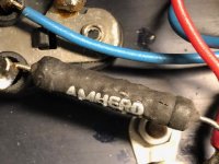
With the amp fully assembled there is not a lot of space for manoeuvre around the circuit board and I am thinking I may have shorted the incoming power supply to the chassis by accident. If that were to happen what do you think would be the first thing to go?
R16 is looking a bit crispy......
Attachments
Last edited:
Evening all,
Today I got to the stage of powering on the amplifier....... nothing blew up!!
I switched the amp on, both power supplies at the same time, there is a very slight buzz from the transformers but you need to have your ear near to the amp to hear it fully. I assume this is normal.
Within around 5 minutes the heatsinks got very toasty.
The first test I did was measure the DC offset at the speaker posts. With my multimeter set at 200mv I got 04.7mV on the right channel and 29.7mV on the left channel.
Such a large inbalance seems odd considering that both channels are now identical in terms of the components used. Is it unusual to have such an inbalance?
Robbie, just a kind pointer for next time: when you switch on for the first time, make sure you have both quiescent current settings dialed down to minimum.
Then, make sure you have a multimeter at each channel to measure the quiescent current, then switch on. If too high, immediately switch off and try to find the issue.
That offset you can investigate at leisure, nothing will break from it, but the quiescent is of utmost importance to prevent toasting the amp.
Jan
- Status
- This old topic is closed. If you want to reopen this topic, contact a moderator using the "Report Post" button.
- Home
- Amplifiers
- Pass Labs
- Nelson Pass A40 Help