I'm not sure if this is the most suitable place to ask this question and I will create a separate thread if need be.
I was going to try and use a few of these boards to make up the filters required for my active 3-way speakers. After taking the SPICE model of the LX mini, copying the individual filter blocks, stacking them and tweaking them I've come up with a response similar to what I'm currently using in DSP.
The problem is I'm using a combination of first and second order filters, stacked to get higher order response. In total 4 high pass and 5 low pass per channel. My speaker designer says specific 4th order filters were not in the original design.
Rather than try to build up multiple boards and attempt to jumper between them all I think going a full custom route is most appropriate.
Which brings me to my questions.
1) How does the correct common drain circuit look using 2 N devices that I would substitute in place of the voltage source that is modeled in SPICE? I'm looking to redraw the circuit in full in a design software and to have my own PCB made, after initial bread board testing of course.
2) I understand the basic board from the store comes with matched JFETS and correct resistors to bias them. Is there a source for just the FETS and resistors? Or if I were to match my own, what are the parameters I should be testing and matching for that would work in this implementation?
If this seems a little ambitious, does anyone know of individual discrete xo boards that are setup for 1st/2nd order HP/LP that I could simply buy as many as I needed and then stuff and stack them to suit.
I appreciate any insight I will ask for further details in another thread to not detract from the LXMini/BIAMPV1 specific discussion. Thanks.
I'm getting better with the search around here and found a bunch of useful info for Jfet unity buffers. Found examples of others who used source followers with ccs. Now its a matter of drawing it and asking for some feedback. Opamps might be good to try first. I will also need to learn a bit more on choosing bias points for Jfets and some finer design tips. It seems getting very low distortion from J113 takes some work. LS fets can be used but will become cost prohibitive on some level as I'll need close to 40 of them.
The filter design is relatively independent of the buffer type, so you can
use a simulated opamp with unity gain instead of worrying about the
jfets. If you want to get picky, the J113 follower gives about 80 ohm
output impedance, which you can insert after the buffer.
It's not what I would call a textbook filter - it is a reasonable duplicate
of the DSP curve Siegfried had, and he suggested the final tweaks on
it through listening.
I have attached it. You can replace the buffer circuitry in simulation
with opamps, or as I do, voltage controlled voltage sources with gain = 1.
Tweaking the J113's is not too difficult. On a clear day you can get some
.00X% numbers at a volt or so. The bias resistors are used to adjust the
current of matched parts down to about 7 mA.
Attachments
Last edited:
Thanks for the reply, Nelson. As mentioned I have taken that circuit already and replaced the buffer with a VCVS in the simulation. I also cut up the individual filters and arranged them to suit my needs.
What I'm just learning are the finer details of JFET matching and biasing.
I'm curious as to what I should be matching for. Should I measure and match all the devices for similar Vp and Idss? If they are to be biased with 7mA I would imagine an Idss a bit higher (8-10mA) would be suitable? Same with 1V of bias that a volt or so higher for pinch off would be correct?
Should I measure and match all the devices for similar Vp and Idss? If they
are to be biased with 7mA I would imagine an Idss a bit higher (8-10mA)
would be suitable?
Generally there is slightly better performance if the Idss is something like
10% higher than operating current, but it's not a big deal.
With two N channels used for a buffer (constant current source +
follower), there are a couple of practical ways of going about it:
1) You match the devices and mate both with the Source resistance
value that sets the current at less than Idss. The advantage here is
that the behavior of the devices offers better cancellation and lower
DC offset. However, the output impedance is higher by the addition
of the resistor on the follower fet.
I often use this with 2SK170/LSK170 as the resistor values can be
fairly low, not degrading output impedance so much, and going for
the lowest distortion, routinely down in the 0.000X% at audio line level.
2) You can use unmatched devices and use the higher Idss part on the
CCS, selecting its Source resistor for slightly less than the Idss of the
follower, and use no Source resistor on the follower, lowering the
output impedance. This has some advantage with higher Idss / lower
transconductance parts such as the J112 / J113. With those parts you
can get 0.00X% numbers.
If you know the load value and have a distortion analyzer, you can
tweak the resistor values for the lowest possible figures (or particular
2nd harmonic). I use a setup with sockets for the Jfets and selectable
resistors, something that DIYers can do and manufacturers do not.
Hi Mr. Pass , I want to build this crossover and I plan to use This Dual Jfet 2SK 194 since I have several pcs. I think no need for them to match. Can I just put this in without changing the values of some resistors? kindly advised.
I plan to use this crossover with my planned set up of Bridged ACA for highs and a Mosfet amp for the Low.
Thanks..
I plan to use this crossover with my planned set up of Bridged ACA for highs and a Mosfet amp for the Low.
Thanks..
Attachments
Hi Junm,
These dual-fets seems almost to nice to be used for line-level followers in a crossover.
If it were me and depending on how many you have, I would try to sell them and see if I couldn't get enough money to buy the analog crossover kit from the Diyaudio store.
Mogens
These dual-fets seems almost to nice to be used for line-level followers in a crossover.
If it were me and depending on how many you have, I would try to sell them and see if I couldn't get enough money to buy the analog crossover kit from the Diyaudio store.
Mogens
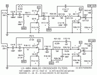
This is a very elegant design and it looks like it could be applied to many other designs.
The Low pass includes a peaked (or not by adjustment) high pass for subsonic rejection
and assisted alignments such as B2=>B4 or B4=>B6, baffle step compensation and a
2nd order low pass. The high pass section is 2nd order with a notch that could be realigned
for stiff cone drivers that require a higher Q notch.
Very nice that it does not require OP amps and uses low cost JFETs.
Is there a circuit board currently available?
Hi Junm,
These dual-fets seems almost to nice to be used for line-level followers in a crossover.
If it were me and depending on how many you have, I would try to sell them and see if I couldn't get enough money to buy the analog crossover kit from the Diyaudio store.
Mogens
I tried to sell those here before but nobody wants it so i decide to use it on my diy projects. I have more than 40 pcs of it but mostly are K grade.
Yes, its in the store under "analog crossover". Topology is correct, just
stuff it with the lx-mini resistors and caps.
I don't see it in the DIYaudio store, perhaps they deleted it?
Hi Nelson
I hope my memory is accurate here.
In an old BAF talk you showed how the circuit could be used as a straight EQ, and you showed the frequency response.
I measured the frequency response of the Loudness button on an old (1994) Pioneer amp. It was virtually a symmetrical smiley face.
Would a loudness circuit be built by simply adding a high q high pass filter and a high q low pass filter or would it be done differently?
I think I prefer the idea of this method more than possibly putting in a broad notch in the mid range. Whenever I have played around with mid range eq even if I have improved the response I have noticed a loss in resolution and detail, I guess our ears are very good at noticing subtle differences in that region.
- Home
- Amplifiers
- Pass Labs
- LX-mini Crossover Article