But keeping unity gain like F4, right?
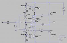
The F7 is (level shifter)->(Gain) and the F4 is (Buffer)->(Buffer).
Check my schematic. I made the first two stages just like the F7. If you look at the F4 you will see that each stage is the inverse of the F7.
The inputs are matched K170/J74 from Punkydawgs.
There are 200 ohm pots in the drains of the input Jfets. Idss of the Jfets is about 8 mA.
Any drawback in using LSK389B?
What's their retail price and how big is variation sample?The LATFETS (...)
I want to use laterals in my version and I want to match them close (to minimize distortion and perhaps avoid degeneration resistors like in XA25.
BTW, can I ask for advice here or you prefer I open another thread (when I'm ready)?
The other main difference for my case is the lower bias since I need only 5 to 10W class A, but I want up to 150W AB on 4ohm.
Any drawback in using LSK389B?
What's their retail price and how big is variation sample?
I want to use laterals in my version and I want to match them close (to minimize distortion and perhaps avoid degeneration resistors like in XA25.
BTW, can I ask for advice here or you prefer I open another thread (when I'm ready)?
The other main difference for my case is the lower bias since I need only 5 to 10W class A, but I want up to 150W AB on 4ohm.
The LSK389 is a dual N channel JFET. Are you thinking of a long tailed pair of NJFETs in the input stage? The F7 uses complementary K170/J74 for the input stage.
I bought some K1058/J162 LATFETs from ampslab.com. The price was USD$45 for 3 N/P pairs. The Vgs at 50 mA is not a match but the F7 has a separate bias control for each LATFET. If you want close matched LATFETs, I think that you would have to purchase a large quantity to get any closely matched parts. I think this is one ingredient of how NP makes great MOSFET amplifiers. He buys large quantities of good transistors and sorts through them to choose matched pairs.
Feel free to ask anything you want to. I am just stumbling through a design here and welcome input.
Thanks, so i'll keep bothering you until you kick me out of your thread ")
Yes, but I think i'll stick with classic K170/J74.
They are a bit expensive, but are exactly the fets I wanna try as well. I have to make some math to see if I need 3 pairs, less or even more (sigh).
And yes, PL has resources and time to match anything they want.
It may not be impossible to find these particular devices already roughly selected from some unofficial source. Gotta recheck the datasheet.
Why did you choose the F7 arrangement? Simplicity? Specs-wise it looks inferior to the F5 to me. Anyway I just need a power buffer, and I dont plan to change anything in the F4 but the output devices and their biasing.
I have looked in the other "f4 beast" thread, ands I found out that besides one prototype with the hockey pucks, the rest are imitations of the xa25 which is not my goal at the moment. The pucks are interesting to me as well and one couple will certainly do, but they seem to require very high bias to be linear, which is against my specsheet.
Why you didn't choose them instead? Just curious eh
An answer like "the latfets probably sounds better" is good enough to me.
The LSK389 is a dual N channel JFET. Are you thinking of a long tailed pair of NJFETs in the input stage? The F7 uses complementary K170/J74 for the input stage.
Yes, but I think i'll stick with classic K170/J74.
I bought some K1058/J162 LATFETs from ampslab.com. The price was USD$45 for 3 N/P pairs. The Vgs at 50 mA is not a match but the F7 has a separate bias control for each LATFET. If you want close matched LATFETs, I think that you would have to purchase a large quantity to get any closely matched parts. I think this is one ingredient of how NP makes great MOSFET amplifiers. He buys large quantities of good transistors and sorts through them to choose matched pairs.
They are a bit expensive, but are exactly the fets I wanna try as well. I have to make some math to see if I need 3 pairs, less or even more (sigh).
And yes, PL has resources and time to match anything they want.
It may not be impossible to find these particular devices already roughly selected from some unofficial source. Gotta recheck the datasheet.
Why did you choose the F7 arrangement? Simplicity? Specs-wise it looks inferior to the F5 to me. Anyway I just need a power buffer, and I dont plan to change anything in the F4 but the output devices and their biasing.
I have looked in the other "f4 beast" thread, ands I found out that besides one prototype with the hockey pucks, the rest are imitations of the xa25 which is not my goal at the moment. The pucks are interesting to me as well and one couple will certainly do, but they seem to require very high bias to be linear, which is against my specsheet.
Why you didn't choose them instead? Just curious eh
An answer like "the latfets probably sounds better" is good enough to me.
Thanks, so i'll keep bothering you until you kick me out of your thread
Yes, but I think i'll stick with classic K170/J74.
They are a bit expensive, but are exactly the fets I wanna try as well. I have to make some math to see if I need 3 pairs, less or even more (sigh).
And yes, PL has resources and time to match anything they want.
It may not be impossible to find these particular devices already roughly selected from some unofficial source. Gotta recheck the datasheet.
Why did you choose the F7 arrangement? Simplicity? Specs-wise it looks inferior to the F5 to me. Anyway I just need a power buffer, and I dont plan to change anything in the F4 but the output devices and their biasing.
I have looked in the other "f4 beast" thread, ands I found out that besides one prototype with the hockey pucks, the rest are imitations of the xa25 which is not my goal at the moment. The pucks are interesting to me as well and one couple will certainly do, but they seem to require very high bias to be linear, which is against my specsheet.
Why you didn't choose them instead? Just curious eh
An answer like "the latfets probably sounds better" is good enough to me.
The top most need in my design is no source resistors and no drain resistors in the output stage. I want unlimited current for short bursts. The hockey pucks seem to be the best devices for this application.
An F7 driving the hockey pucks is simpler than the F5 driving the pucks. In fact, if I understand NP's F7 manual, the F7 is the simplest distillation of the F5. I like simple and I like that the F7 has no capacitors.
Yes, the pucks seem current monsters indeed, and you understand the F7 schematic correctly (and better than me anyway).
I see your reasoning, dropping resistors should help for current bursts.
Go on, I'm following your project
Are your ribbons "fullrange"? In the past I have looked to ribbons for midrange use, that could go as low as 300hz, maybe open back, with no luck.
My ribbons are line source tweeters. Definitely not midrange. For midrange I have a stash of ancient Audax Bextrene 5 1/4" drivers to be used as a line source.
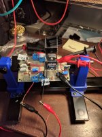
The input stage is soldered and running. The Idss of the JFETs are 8mA and this input stage runs at 6mA.
The 6mA idle bias caused me to add two resistors, R17 and R18. R17 allows 0.6 Vgs on M2 with the 100 ohm pot at closer to its center rather than at one of its extremes.
R18 was added to balance the total drain resistances of both N and P JFETs.
The driver stage should be up and running by the end of this weekend.
The bias spreader is working on the bench. The bias spreader has a negative temperature coefficient. As it warms up, Vds decreases while at 50mA constant current.
Attachments
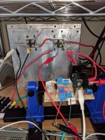
The driver board is up and running. 6mA Ids though each JFET. 49mA bias through the LATFETs and bias spreader. 7V across the bias spreader.
I added a 1 ohm resistor in series with each JFET and one right next to the bias spreader. This allows measuring current in both stages.
I added a 1 ohm resistor in series with each JFET and one right next to the bias spreader. This allows measuring current in both stages.
Attachments
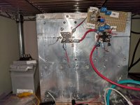
Here is the entire amp together and running. Input stage 6mA, LATFETs 50mA and OPS something like 200mA. This is just to look at bias stability and output offset.
Output offset is not very stable. It wanders around 100mV or so. I am guessing that adding negative feedback will stabilize the output DC offset.
Later in the weekend, I will connect a sig gen and scope to measure open loop gain and bandwidth as well as look at output impedance.
Output offset is not very stable. It wanders around 100mV or so. I am guessing that adding negative feedback will stabilize the output DC offset.
Later in the weekend, I will connect a sig gen and scope to measure open loop gain and bandwidth as well as look at output impedance.
Attachments
Looks good. Maybe, latfets sharing the same heatsink wood help a bit with the offset. Input jfets facing each other too.
Agreed. That will require a custom board layout to get the LATFETs on the edge of the PCB and have the JFETs facing each other.
I purposely left almost all of the FETs' legs above the PCB so that I could clip them to move to a better PCB.
Hi Woofertester,
Would the K213/J76 be better fit in the second stage, considering the chosen bias?
Prakit
It will have to wait for some measurements to see if the LATFETs can drive the pucks well. I used them because I had some already in hand and I know that they can drive speakers.
Fired up the sig gen and scope.
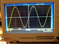
Open loop gain at 1 kHz is 70X. 7v p-p out, 100 mV p-p input. Scope shot is at 7V p-p out.
Open loop bandwidth at -3dB is about 21 kHz.
These measurement are with a 47 ohm load.
Bias wanders 100mV or more at rest. Bias wanders quite a bit more while powering the dummy load.
Clipped amplitude is about 40V p-p into 47 ohms.
Attachments
Open loop bandwidth at -3dB is about 21 kHz.
This is low.
This is low.
The specs for the XA25 state -2dB at 100kHz.
When feedback is applied to my amp, if I get something close to -2dB at 100 kHz, I will be thrilled.
- Status
- This old topic is closed. If you want to reopen this topic, contact a moderator using the "Report Post" button.
- Home
- Amplifiers
- Pass Labs
- F4 Beast with hundreds of amperes