For my next Whammy (number 4), I'm planning to use a Khozmo pot, which can't be soldered on anyway. It occurred to me that, in that case, I can bypass the initial connection to the PCB and those traces just connect the input wires to the pot.
But there's also the 2.2K input resistor. Is that essential? What is it there for? Of course, I could still include it right in front of the pot, but I'm curious anyway.
Not essential in many instances. I would leave the 1K after the pot for stability.
You don't even need the input cap if you really know your source has no DC.
Thanks, Wayne. I'll go ahead and build it without R39 and R40 and see how it goes. Easy enough to add them later.
This particular Whammy will use the best parts I can find, just to see how good it can get. The resistors in the signal path are all Caddock and Vishay Naked Z-Foil. The coupling caps, which I'll keep for now, are Jantzen Silver, with Nichicon FGs elsewhere. I'm using the New Class D regulators and the Khozmo pot.
We'll see whether all that makes a difference, but it'll look nice!
I modeled the ripples of a drip of water in CAD and then CNC milled the walnut.
I thought it was a speaker cone vibrating!
How do you determine whether or not your source has DC?Not essential in many instances. I would leave the 1K after the pot for stability.
You don't even need the input cap if you really know your source has no DC.
The build guide has instructions for this. Though, if it's already built, you may not be able to access those points. In any event, (one side of) R10 and R14 should work. You will find ground in many places, e.g., one side of R9 or D5.
") not sure how missed that as I'm sure it's what I did when I first built it. Doh!
not sure how missed that as I'm sure it's what I did when I first built it. Doh!I didn't really take any pics of the build itself. I realize now that I should have! The walls are pocketed on the insides so that I could put through holes in the pocket walls for screws that then mate to tapped holes in the other panels. The board is mounted on standoffs "upside down" to the top of the case. The bottom comes off with 4 screws for easy access to everything. I also cut mounting parts for the switches and headphone jack that mount to the inside of the end panels so that everything can be cleanly mounted so no nuts are visible from the outside.
I cut all the parts on a 3 axis CNC. It's a Hurco.
Interesting idea mounting the board upside down, I considered that but was a little bit worried about heat. It should be fine though as many people have built without any vent holes at all.
Any photos of the interior would be cool to see if you have any.
High Noise Floor
I need some help.
I changed all the signal path caps a couple of months ago (to Audio Note) and now I have a higher noise floor on some op amps. All the values on the new caps are same as the original design.
Using OPA2107, the noise floor apperas to be the same as before. Using AD823, the noise is much higher. With sensitive headphones like Focal, it's almost unusable. Any idea what has caused this?
My rails are -16.92V and 16.75V. Offset on the AD823 is 0.1mV on the right and 0.3mV on the left.
I always wished this amp had a lower noise floor in general but that's a different story.
Last edited:
So, I'm not all that experienced with this stuff, so you've probably already thought of these things. But just in case....
There is that remark on the schematic about some op-amps being liable to misbehave in some circumstances. Even though the values of the caps are the same, could something weird have changed in how the AD is behaving? Maybe try C2 and C7?
The other obvious thing is that maybe it's actually the op-amp that's the problem.
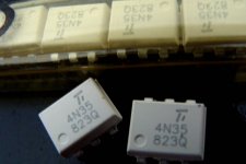

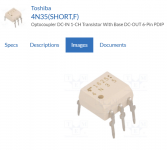
I did a google image search for 4N35 and the pictures of TOSHIBA 4N35s seem to match the photo in #3892. Toshiba has exited the optoelectronics business, those parts are old. You won't find Toshiba 4N35s for sale today on Mouser.com or Digikey.com or Element14
_
_
Attachments
Question for all of you who have built this, has anyone had any issues with some of the pads on the PCB?
I have had a couple of spots where the solder just doesn't want to stick. I have tried cleaning the are with both isopropyl and acetone, sanding the are if any of the solder mask has melted, more heat, less heat, more flux, no extra flux yet some components just doesn't want to be soldered to the PCB.
Any advice is greatly appriciated before I start to desolder the components and order a new board.
Question for all of you who have built this, has anyone had any issues with some of the pads on the PCB?
I have had a couple of spots where the solder just doesn't want to stick. I have tried cleaning the are with both isopropyl and acetone, sanding the are if any of the solder mask has melted, more heat, less heat, more flux, no extra flux yet some components just doesn't want to be soldered to the PCB.
Any advice is greatly appriciated before I start to desolder the components and order a new board.
Are those positions at the ground plane? Do you have more photos?
Ground pads are harder to solder because the copper mass becomes a heatsink during soldering.
I need some help.
I changed all the signal path caps a couple of months ago (to Audio Note) and now I have a higher noise floor on some op amps. All the values on the new caps are same as the original design.
Using OPA2107, the noise floor apperas to be the same as before. Using AD823, the noise is much higher. With sensitive headphones like Focal, it's almost unusable. Any idea what has caused this?
My rails are -16.92V and 16.75V. Offset on the AD823 is 0.1mV on the right and 0.3mV on the left.
I always wished this amp had a lower noise floor in general but that's a different story.
Some of the OpAmps are particularly fussy about the ESR of the caps right around them. I know the SparkOS ones have application notes to this affect, for example. Or the Bursons need the .1uF rail bypasses. While the OpAmps are pin-swappable, they may need some modifications to the circuit around them if you do.
I need some help.
I changed all the signal path caps a couple of months ago (to Audio Note) and now I have a higher noise floor on some op amps. All the values on the new caps are same as the original design.
Using OPA2107, the noise floor apperas to be the same as before. Using AD823, the noise is much higher. With sensitive headphones like Focal, it's almost unusable. Any idea what has caused this?
My rails are -16.92V and 16.75V. Offset on the AD823 is 0.1mV on the right and 0.3mV on the left.
I always wished this amp had a lower noise floor in general but that's a different story.
Are those positions at the ground plane? Do you have more photos?
Ground pads are harder to solder because the copper mass becomes a heatsink during soldering.
Have you tried applying some solder flux to the pads? Your iron might not be hot enough and/or not recovering well when you touch the pads. All of these problems were solved for me when I started using The Fire Metall solder from the store. Richard has done a fantastic job tuning the recipe in to the point where its the only solder I use.
--Tom
- Home
- Amplifiers
- Pass Labs
- "WHAMMY" Pass DIY headphone amp guide