I wish to open a new thread to discuss auto-biasing circuits for MOSFETs and BJTs, e.g. in the complementary source follower or emitter follower.
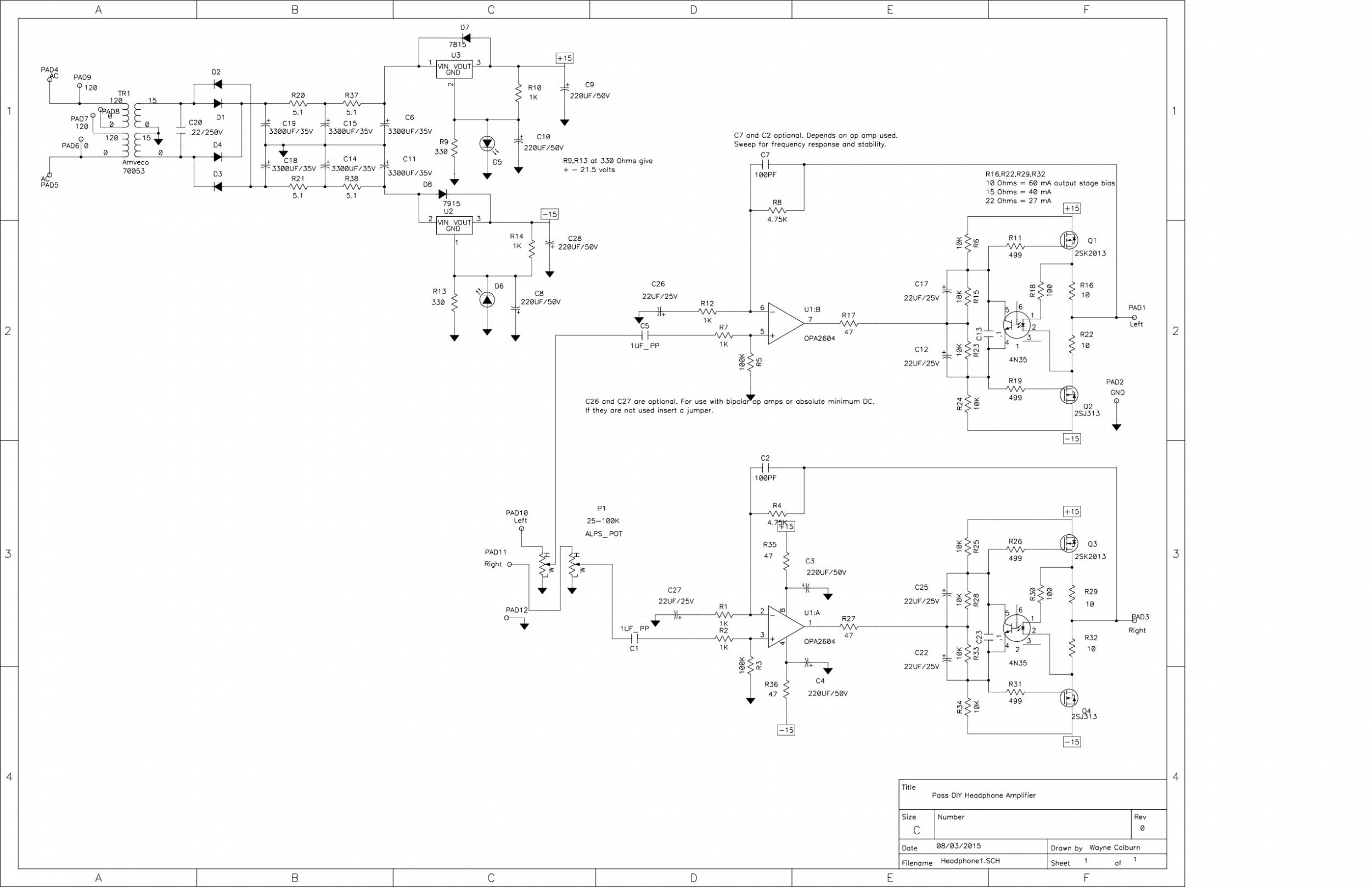
Examples can be found in the FW M2 and the Pass DIY Headphone Amp.
All thanks to Nelson and Wayne for sharing with us their idea of using an opto-coupler in their self-biasing circuit.
http://www.diyaudio.com/forums/atta...5d1445746020-official-m2-schematic-m2-sch-gif
http://www.diyaudio.com/archive/gallery/data/500/WhammyFULLrev1.jpg
Class A or AB Complementary Followers are of course nothing new.
Mostly their bias is set using simple potential dividers connected to the top and bottom rails, or resistor (or CCS) biased diodes.
Often, additional capacitors are included in parallel with the biasing element.
HeadWize - Project: Designing an Opamp Headphone Amplifier (A HeadWize Design Series Paper)
Fig. 11
Headphones, amplifiers, and virtual grounds | Electronics Forum (Circuits, Projects and Microcontrollers)
Post #8
A key disadvantage of these simple, fixed-voltage biasing circuits is that they do not account for the temperature coefficient of the Vgs or Vbe of the output devices.
Should the latter have a positive tempco, the bias will increase with temperature.
The "cure" is of course generously sized heat sink and power supply, and the inclusion of a emitter / source resistor which reduces this change in bias current.
The Pass circuit also uses a potential divider, with a nominal voltage set to a much higher value (e.g. < 5V) than actually required.
This is then regulated by sensing the bias current through the source resistor using an opto-coupler, and using the latter to reduce the biasing voltage to the desired value.
In the Pass circuit, a single opto-coupler is used across both source resistors.
Thus it is the sum of current of the top and bottom power device that is being regulated by the opto-coupler.
In the absence of any output current, this is of course 2x I_bias.
There have been of course other self-biasing circuits being employed over the years.
I hope that we can perhaps have an open discussion of the subject.
And perhaps Nelson and Wayne can shed some light on the reasoning behind their particular design choice.
One example of a classic self-biasing circuit can be found in the headphone amplifier circuit published by John Linsley Hood in 1985.
A Paul Kemble web page - John Linsley Hood preamp designs.
Instead of using a single opto-coupler, John used a pair of complementary BJTs as the current regulating element.
The circuit had some resemblance to the current limiter in the FW F5 Power Amp, but used a R-C LP filter of 0.16Hz to restrict the current regulation to DC only.
I have included here a version applied to a complementary emitter follower, for a more direct comparison.
Patrick
.
Attachments
To demonstrate the versatility, here the same circuit using Fairchild MOSFETs.
The source resistors R13,14 have been reduced to 4R7 as MOSFETs need more bias to sound good, IMHO.
But it still works well with R10, if one wishes to save power.
One can of course substitute any other power output combination, such as IRF610/9610.
And they do not even need to have the same Vgs at bias.
Patrick
.
Attachments
And thermal coupling of the bias spreader semis to the output's.... A key disadvantage of these simple, fixed-voltage biasing circuits is that they do not account for the temperature coefficient of the Vgs or Vbe of the output devices.
Should the latter have a positive tempco, the bias will increase with temperature.
The "cure"� is of course generously sized heat sink and power supply, and the inclusion of a emitter / source resistor which reduces this change in bias current. ...
I also think some background information on Nelson's and Wayne's choice of component for the opto autobias would be invaluable.
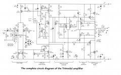
No one has mentioned the biasing in the Signal Transfer Company TriModal amplifier, schematic below. It uses transistors TR14-TR17 to measure the voltage dropped across the emitter resistors of an output push-pull pair. This is compared against a zero-tempco reference voltage supplied by a bandgap shunt regulator IC named "RG1". Output stage bias is adjusted up or down as needed, to keep the emitter resistor voltage drop at a constant value.
I expect the temperature coefficient of an optoisolator's LED forward voltage drop, is not as well controlled or well characterized, as the temperature coefficient of an LM385-1.2 bandgap IC.
_
I expect the temperature coefficient of an optoisolator's LED forward voltage drop, is not as well controlled or well characterized, as the temperature coefficient of an LM385-1.2 bandgap IC.
_
Attachments
And perhaps Nelson and Wayne can shed some light on the reasoning behind their particular design choice.
Bias circuits have always been a subject of exploration, from the dynamic
bias of the 800A, 400A and 4000 and later the patented optically controlled
bias for Threshold. And there was the DIY A40 amplifier.
As I was leaving Threshold, I left them with a new bias circuit which my
replacement did not see fit to implement. Bad luck for them.
Routinely the trick is not that of setting the bias, but preventing the value
from being disturbed by output currents greater than twice the idle current.
This was solved nicely in the First Watt M2. Still, this approach required
sensing of current across the Source resistors, so about 8 years ago I
developed an autobias circuit which senses elsewhere, allowing the output
stage to operate without Source degeneration, and this is found in the
XA-25, currently the subject of reviews in the magazines and online.
At this time the bias circuits are now good enough, and my attention is
elsewhere.
")
what about the TL431 method of F4 BA?
That is biasing with a constant voltage reference. I think we have been
talking about bias circuits that adjust themselves.
One of the most troublesome of current sensing aspect is the unavoidable addition of a resistor right in the path where usually resistance as small as possible is preferred.
Since price of hall effect sensors are quite affordable and will only add mili Ω for sensing eg. 0.65 mΩ for ACS723. With all the talk and effort on low PSU resistance and elimination of source degeneration I think they offer a good alternative for autobias circuits. I have not seen anybody refer to them here in Papaland. Are they any good? Is there a catch we need to be aware of? Anybody interested in having a discussion on them here, or better on the beast thread?
Since price of hall effect sensors are quite affordable and will only add mili Ω for sensing eg. 0.65 mΩ for ACS723. With all the talk and effort on low PSU resistance and elimination of source degeneration I think they offer a good alternative for autobias circuits. I have not seen anybody refer to them here in Papaland. Are they any good? Is there a catch we need to be aware of? Anybody interested in having a discussion on them here, or better on the beast thread?

Since the optocoupler only senses positive current Dosnt the bias change with signal?
No if the bias is high enough like in the DIY headphone amp. You also have big caps around the opto and Nelson has some other tricks.
- Status
- This old topic is closed. If you want to reopen this topic, contact a moderator using the "Report Post" button.
- Home
- Amplifiers
- Pass Labs
- Auto-Biasing Circuits for Complementary Followers