You don't want permalloy for the gauss/belly band.........................
i am still waiting for a permalloy strip to wrap around,..............
Ordinary mild steel, or other high ferrous content iron will do perfectly well. The thicker the better.
How did you do this?but i have added a screen winding between primary and secondary.
240 is perfectly OK.I will begin to design the regulator pcb, i think i will go with irfp240/9240 as active elements, i think there are better choices out there... but i am not aware of
there are many vertical mosFETs that work well in audio amplifiers and of these the 240 are well recommended. There are a few that are specifically designed for audio output stages, but they tend to be very expensive in comparison to 240 and give a small benefit if incorporated into a design that gets the best out of them.
Look up R.Cordell's mosFET Power Amp, which uses ordinary switch mode vertical mosFETs for exemplary performance as a linear audio amplifier.
How did you do this?
They are used to put a very tight small gauge winding all around the primary and then connect only one end.
I start wondering about its effectivness.
That sounds odd.
An interwinding screen is normally a screen layer (probably aluminium) wrapped around the primary but insulated so that it cannot form a shorted turn.
That is then connected to the enclosure.
The secondary is then wound around the screening layer.
This forms a C Screen C double capacitance between the three components.
The first C is shunted by a low inductance wire to enclosure and acts as an LC+RC filter to take some of the mains interference to the chassis.
The remaining interference that is not fully attenuated to taken via the second C to the secondary.
I cannot see an inter-winding wire (with lots of inductance) achieving much C filtering.
I think you are totally right about that.That sounds odd.
An interwinding screen is normally a screen layer (probably aluminium) wrapped around the primary but insulated so that it cannot form a shorted turn.
That is then connected to the enclosure.
The secondary is then wound around the screening layer.
This forms a C Screen C double capacitance between the three components.
The first C is shunted by a low inductance wire to enclosure and acts as an LC+RC filter to take some of the mains interference to the chassis.
The remaining interference that is not fully attenuated to taken via the second C to the secondary.
I cannot see an inter-winding wire (with lots of inductance) achieving much C filtering.
I don't know why, but they have did this way for a very long time, maybe is less effective or more easy to manage for them.
I think at this point is stupid to take out the secondary winding to redo the electrostatic shielding with a copper/alluminium foil.
If it makes more damage than good i will keep it disconnected.
For the belly shielding i have taken a roll of the same material they use for the toroidal core itself, i am going to wrap around as many times i can to increase the thickness. (the foil is 0.5mm thick).
Compare to a N.Pass Zener+Follower PSU.This is the regulator i am evaluating to put in use.
irfp240/irfp9240 as pass elements.
Do you think is it suitable ? Simulated with a 4 amp constant load and it seems fine.
Compare to a N.Pass Zener+Follower PSU.
I have taken the schematic from the Zen v3 PSU.
my only concern is about filtering,
i have planned to use 22mf after bridge and 22mf after regulator.
so CRegC => 22mf -> ZenV3 -> 22mf. One for each half supply.
From simulations the output ripple is almost absent, and at the input is around 2Vptp (with 4A costant current load).
I don't know how much transients loads the capacitors/regulator. Maybe i need to add up some more capacitance in the output ? For sure i will put as much as possible of it close to the output devices.
For the rectifier bridge i also paln to "recycle" the same MUR3020 that we need in the output stage. I think the parameters are fine to support this workload.
Little update.
Today has arrived all the MUR3020 didoes, low power resistors (Royal Ohm), source degeneration resistors (Vishay, i will match them to be equal as possible) cascode BJTs (SA1837 / SC4793) and other minor parts.
I have made some measurements on the real transformers.
and i got 50.5v [DC] loaded with 3 ampere (used an electronic load).
in this situation, with only 22mf of filtering after bridge i got ~850mVpp.
I fear that the regulator (inspired by Zenv3) will dissipate too much and maybe the "easy" way is to filter the ripple with a stronger capacitor bank + LC filtering.
Said that less ripple is always the best, in your experience with thoose topology how much of the PSRR i would expect ? in other words, there a safe "threshold" of ripple to avoid too much noise in the output ?
Hi guys,
still waiting for the pcb to arrive....
I am making some cam program for my hurco to make pockets, hole, threads for all the mosfets and pcbs...
any advice on where to put the thermistor ? i got that is for reducing thermal drift, but i have seen a lot of pictures where many users puts them either straight over mosfet of other over the pcb...
Can you advice a good spot to mount them ?
Thanks
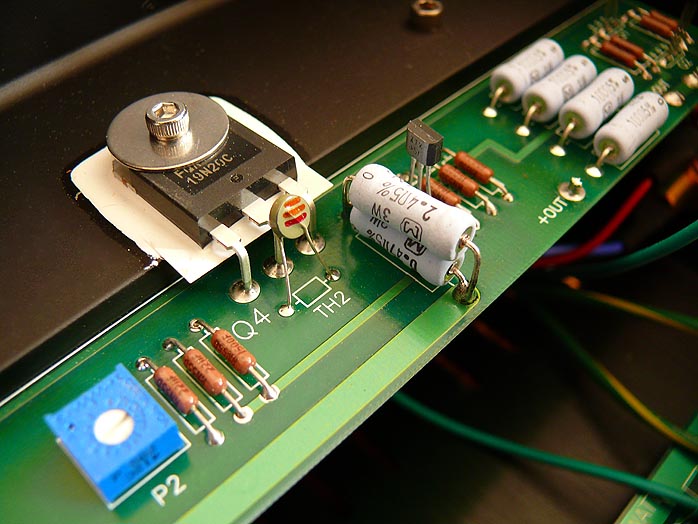
you know for any picture of Papa's F5T ?
... mhhh only from other users, maybe i've missed something important

as usual , there are plenty of details to learn , just looking at pictures of origin
in a meantime , as you're searching for either F5 or F5T origin pictures , place body of NTC right against ceramic part of mosfet body
take care that legs of NTC are well away of any metal part , or even better - insulate them.
in a meantime , as you're searching for either F5 or F5T origin pictures , place body of NTC right against ceramic part of mosfet body
take care that legs of NTC are well away of any metal part , or even better - insulate them.
as usual , there are plenty of details to learn , just looking at pictures of origin
in a meantime , as you're searching for either F5 or F5T origin pictures , place body of NTC right against ceramic part of mosfet body
take care that legs of NTC are well away of any metal part , or even better - insulate them.
There's need to clamp it on the ceramic, or is just enough to bend the insulated legs against the mosfet ?
bend legs to lean NTC to ceramic part of mosfet
as you can see on pictures here : 6moons audio reviews: FirstWatt F5 , Pa is putting NTC in proximity of mosfet mid pin ; that's convenient enough , with his pcb and parts arrangement (Him - being Founder of FAB Club)
I don't know which pcbs are you using and where exactly NTCs are situated , but you can always extend NTC legs ( heatshrink!!)
wherever you put NTC , difference is just in biasing behavior in time domain ....... more intimate thermal bond of NTC with mosfet case/surround is resulting in lesser and faster Iq change
though , ceramic part of mosfet case is most secure position ....... not one F5 gone Dodo , due to poor NTC going nude in hostile environment
 http://www.6moons.com/audioreviews/firstwatt7/2_7.jpg
as you can see on pictures here : 6moons audio reviews: FirstWatt F5 , Pa is putting NTC in proximity of mosfet mid pin ; that's convenient enough , with his pcb and parts arrangement (Him - being Founder of FAB Club)
I don't know which pcbs are you using and where exactly NTCs are situated , but you can always extend NTC legs ( heatshrink!!)
wherever you put NTC , difference is just in biasing behavior in time domain ....... more intimate thermal bond of NTC with mosfet case/surround is resulting in lesser and faster Iq change
though , ceramic part of mosfet case is most secure position ....... not one F5 gone Dodo , due to poor NTC going nude in hostile environment
Last edited:
bend legs to lean NTC to ceramic part of mosfet
as you can see on pictures here : 6moons audio reviews: FirstWatt F5 , Pa is putting NTC in proximity of mosfet mid pin ; that's convenient enough , with his pcb and parts arrangement (Him - being Founder of FAB Club)
I don't know which pcbs are you using and where exactly NTCs are situated , but you can always extend NTC legs ( heatshrink!!)
wherever you put NTC , difference is just in biasing behavior in time domain ....... more intimate thermal bond of NTC with mosfet case/surround is resulting in lesser and faster Iq change
though , ceramic part of mosfet case is most secure position ....... not one F5 gone Dodo , due to poor NTC going nude in hostile environment
Perfect, got it.
Today i have ordered to a local company 4x inductors, 1mH / 0.04Ω rated for 10A. They'll make on a toroidal iron core.
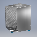
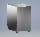
The main PCB was stuffed with all the components, and this weekend i will CNC-drill all the holes on the heatsinks so i can start attaching the boards and start some preliminary tests.
The finished case form-factor will be something like the images attached.
Wish me luck
Attachments
Last edited:
some days are passed. And i still trying to recover from a bad flu.
Next step will be the machining of the heatsink, so i can finally attach the mosfets and start tuning the system.
In the meantime i have received previous ordered inductances of 2mH 10A.
i start planning the power supply for the tests.
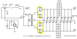
I have on hand a 1400VA toroid with 230v input and 2x38Vac secondaries.
I have made some pcbs to mount the same MUR3020 i use on the channel for rectification... and my idea is to make a 38-0-38 Center tap, with dual bridge and then 44mF+2mH+44mF each rail. this will end up in something like 55Vdc unloaded.
What do you think about this arrangement ?
There are advantages (from your honorable experiences) in using a 0-38 + 0-38 with dual bridge over a center tapped solution ?
Next step will be the machining of the heatsink, so i can finally attach the mosfets and start tuning the system.
In the meantime i have received previous ordered inductances of 2mH 10A.
i start planning the power supply for the tests.
I have on hand a 1400VA toroid with 230v input and 2x38Vac secondaries.
I have made some pcbs to mount the same MUR3020 i use on the channel for rectification... and my idea is to make a 38-0-38 Center tap, with dual bridge and then 44mF+2mH+44mF each rail. this will end up in something like 55Vdc unloaded.
What do you think about this arrangement ?
There are advantages (from your honorable experiences) in using a 0-38 + 0-38 with dual bridge over a center tapped solution ?
Attachments
Last edited:
some days are passed. And i still trying to recover from a bad flu.
Next step will be the machining of the heatsink, so i can finally attach the mosfets and start tuning the system.
In the meantime i have received previous ordered inductances of 2mH 10A.
i start planning the power supply for the tests.
I have on hand a 1400VA toroid with 230v input and 2x38Vac secondaries.
I have made some pcbs to mount the same MUR3020 i use on the channel for rectification... and my idea is to make a 38-0-38 Center tap, with dual bridge and then 44mF+2mH+44mF each rail. this will end up in something like 55Vdc unloaded.
What do you think about this arrangement ?
There are advantages (from your honorable experiences) in using a 0-38 + 0-38 with dual bridge over a center tapped solution ?
anyone ?
Attachments

- Status
- This old topic is closed. If you want to reopen this topic, contact a moderator using the "Report Post" button.
- Home
- Amplifiers
- Pass Labs
- Y.A.F5Tv3.B.T. Yet another F5Tv3 Build Thread