I tried setting counterclockwise P3 and P4, and that doesn't change anything,
I verified the way I connected Q7 and Q8 and it seems OK. Finally I compared my work to the schematic instead the Supplemental kit list BOM (as i did because convenient!)
I found Q5 = 2SJ313 P chanel
Q6 = 2SK2013 N chanel
but in the Supplemental kit list
Q5 = 3N30 N chanel
Q6 = 3P20 P chanel
I'm wondering if the fact of having inverted them they can have been damaged? or is ok and i have just to switch them?
I tried setting counterclockwise P3 and P4, and that doesn't change anything,
I verified the way I connected Q7 and Q8 and it seems OK. Finally I compared my work to the schematic instead the Supplemental kit list BOM (as i did because convenient!)
I found Q5 = 2SJ313 P chanel
Q6 = 2SK2013 N chanel
but in the Supplemental kit list
Q5 = 3N30 N chanel
Q6 = 3P20 P chanel
I'm wondering if the fact of having inverted them they can have been damaged? or is ok and i have just to switch them?
Yes I think an early version of the BOM had an error like this in it.
Corrected BOM in post #2766 of the DIY Sony VFET pt2 thread: http://www.diyaudio.com/forums/pass-labs/276711-sony-vfet-amplifier-2-a-277.html#post4991406
On the pcb Q5 (left position) is supposed to be P channel, so either 2SJ313 or FQP3P20. Q6 (right position) is supposed to be N channel, so either 2SK2013 or FQP3N30.
On the pcb Q5 (left position) is supposed to be P channel, so either 2SJ313 or FQP3P20. Q6 (right position) is supposed to be N channel, so either 2SK2013 or FQP3N30.
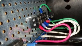
tidy up that CL60
I think the CL60 is where GND meets PE. Not deadly, bit still not pretty, I agree.
I switched Q5 and Q6 in my boards , one works fine but the other one I have to replace them
I mesured the voltage and I get 4v through T6-T7 and T8-T9 !
G-T6. +29
G-T4 -23.84
T6-T7 +4.07
T6-T11 +27.80
G-T14 +1.24
G-T19. +11.65
G-T17. +8.34
G-T8. +29.39
G-T2. +24.06
T8-T9. -4.03
T8-T13 +28.94
G-T15. -0.35
G-T20. -13.80
G-T16. -12.72
I don't know what to do at this point!
I mesured the voltage and I get 4v through T6-T7 and T8-T9 !
G-T6. +29
G-T4 -23.84
T6-T7 +4.07
T6-T11 +27.80
G-T14 +1.24
G-T19. +11.65
G-T17. +8.34
G-T8. +29.39
G-T2. +24.06
T8-T9. -4.03
T8-T13 +28.94
G-T15. -0.35
G-T20. -13.80
G-T16. -12.72
I don't know what to do at this point!
T14 and T15 would suggest that the input jfets are not turned on, thus not passing any current and not dropping any voltage over the resistor and pot. What jfets are you using? Where were they sourced and are they installed correctly? Are Q3 and Q4 populated correctly (Q3 NPN BC550 and Q4 PNP BC560)? Also check R7 to R7 for correct value.
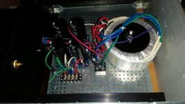
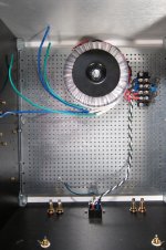
How have you insulated the bottom of the PSU PCB it looks to be mounted very close to the bottom of the chassis, & do you have a fuse anywhere? Also is that orange cap safety rated, I've never seen one in that collour? If not, if it shorts you'll have a problem.
Last edited:
Hi Folks,
I constructed the PSU exactly as shown here:
A guide to building the Pass F4 amplifier.
The photos of the power supply are at a bad angle. It's about 1/4" off the board. Tall enough that the 2.2k bleeders are under it, but each still about 1/8" off the base plate.
I want it to be safe and correct, but don't see where/how to change the connection to chassis ground. The side of the CL60 that is attached to the chassis is connected to earth through the schurter power inlet. Same one as comes with the back panel kit in the store.
All help is appreciated")
I constructed the PSU exactly as shown here:
A guide to building the Pass F4 amplifier.
The photos of the power supply are at a bad angle. It's about 1/4" off the board. Tall enough that the 2.2k bleeders are under it, but each still about 1/8" off the base plate.
I want it to be safe and correct, but don't see where/how to change the connection to chassis ground. The side of the CL60 that is attached to the chassis is connected to earth through the schurter power inlet. Same one as comes with the back panel kit in the store.
All help is appreciated
- Home
- Amplifiers
- Pass Labs
- Sony vFET Illustrated build guide