Nice! I will keep my eye out for the schematic")
I guess the difference is bigger with a hard to drive power amp/power amp with low input impedance. That is however my case.
Also, note my Toshibas are extremely well matched. With 1mA discrepancy the DC offset will be very large, I expect.
Also, the circuit requires a power amp with a cap on the input.
Will also test with the AJ, in time. But it had a much higher input impedance, so perhaps not as notable results there. Will see
.......
Also, the circuit requires a power amp with a cap on the input.
.......


what's wrong with some brain activity, here and there?
regular DC coupled amp is having - what - 15 to 25V/V gain;
if you inject 2mV in input of amp like that, you get 30 to 50mV at output
I see no reason for above declaration

Pico insisted on that caveat. For example, how many of us have toshibas matched within 0,01mA? Some of course, but batches of that similarity are likely very few.
what's wrong with some brain activity, here and there?
regular DC coupled amp is having - what - 15 to 25V/V gain;
if you inject 2mV in input of amp like that, you get 30 to 50mV at output
I see no reason for above declaration
So it is not a circuit for everyone, I would say.
But in my specific case, yes, I could do without.
But I do agree, to the extent that my declaration was innacurate: unless you have very well matched JFETs, ensure an amp with that takes care of the possibly high DC offset. So yes, you are right - as always

I knowWeaklingsesss are using it without proper shunt reg

And with resistive attenuator? What is the world coming to
what's wrong with some brain activity, here and there?
regular DC coupled amp is having - what - 15 to 25V/V gain;
if you inject 2mV in input of amp like that, you get 30 to 50mV at output
I see no reason for above declaration
Really just being ultra conservative for a first dip into this water, don't want to throw people in the deep end of the FAB pool, without some floaties.
Mostly concerned with potential thermal drift, what might start out 2mV might end up being 15mV etc, then there are people who don't have airconditioning so things could be quite different between summer and winter in someone's home.
Just want to be sure people have a good experience with this, before they get more adventurous.
A couple of thoughts. It may be a good idea to put the B1 R2'moded in a sealed case similar to how the B1 Korg is in so airflow etc can't influence it. Could also tie the two JFETs together like how it is done on the F6 so that they are more thermally stable.
You could put your fingers on one of the JFETs to get them to be thermally different. Then you could see get an idea of how big of an issue this is.
You could put your fingers on one of the JFETs to get them to be thermally different. Then you could see get an idea of how big of an issue this is.
These are all reasonable ideas, but the parts themselves generate their own heat and have a temperature coefficient to be mindful of.
I'm not too concerned about having the parts thermally coupled together, more about changes in ambient temeperature etc.
Coupling the parts together keeps both parts near the same temperature, but it does not control the min/max temperature drift that I am thinking of.
Every best solution will be unique to the operating environment of each builder.
Anyway, we're probably overstating how significant the issue is, but we should still be mindful of it.
Well, based on the last few posts I stress tested the circuit wrt temperature differences today.
In approx 18 degrees C ambient, offset is 1,3mV and 2mV respectively.
After 30 seconds blowing with a maxed out hair dryer, offset drifted approx 2mV, towards negative. So the 2mV left channel offset in fact zeroed out.
So I guess this FAB B1 is conceptually proven, for now
Blowing on the circuit/JFETs with my mouth, and or touching the jfet cases, had minimal effect. Like initially seen, a very stable circuit.
I like seeing the interest in this buffer since it is my primary means of controlling volume with my horns. My question is why hasn't the store a board available to build this buffer? Simple enough to build on a proto board but a readily available board would be an assent in the store.
The store has the DCB1. Pass Labs website sell the B1 R2 (non complimentary) version, with K170’s and it is a great deal.I like seeing the interest in this buffer since it is my primary means of controlling volume with my horns. My question is why hasn't the store a board available to build this buffer? Simple enough to build on a proto board but a readily available board would be an assent in the store.
Soon the store hopefully will have Mighty’s Iron Pre, a FAB/GBC B1-inspired pre with shuntregs on board
and optional transformer gain.
Last edited:
I now understand why not. We do not want to step on any toes especially the boss'.Pass Labs website sell the B1 R2 (non complimentary) version, with K170’s and it is a great deal.
To speed up the response time, I am happy to answer.
This looks good to me.
It might be worth adding a place for an output resistor that people could solder a link in if they didn’t want a resistor.
Andy may not want that but it’s good to have some options.
This looks good to me.
It might be worth adding a place for an output resistor that people could solder a link in if they didn’t want a resistor.
Andy may not want that but it’s good to have some options.
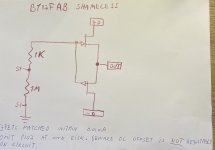
Cool. Maybe something like this would be handy:

Looking at the left side, you can use P1 to figure out what resistance would be needed for R3 and R4. Then you could jump P1 out of the signal path. And jump R5 if you wanted to.

Mock up board layout. The GND pad is just an easy place to put your probe. It can be ran dual mono.

Do you think the resistors to bypass the pot on JFETs that aren't matched to .01ma are worthwhile?
Looking at the left side, you can use P1 to figure out what resistance would be needed for R3 and R4. Then you could jump P1 out of the signal path. And jump R5 if you wanted to.
Mock up board layout. The GND pad is just an easy place to put your probe. It can be ran dual mono.
Do you think the resistors to bypass the pot on JFETs that aren't matched to .01ma are worthwhile?
- Home
- Amplifiers
- Pass Labs
- B1 Rev. 2