OK, I had mistakenly assumed that you were aiming for something similar to the XA25 which is good for 200W peak into 2 ohms.
Does this also mean that you are not interested in a frequency response down to DC (as per XA25)? Although C1 and C2 are large in your circuit, the output will still reduce at lower frequencies. Although I suspect that most of us will not wish to operate our amplifiers at DC, it is still an interesting challenge to solve.
The XA25 spec is 200W peak into 2R, but that is class AB. It will do 50W peak class-A.
Last edited:
Refresh my last post. It should have said:Is there a missing "not" in there? If the 200w into 2 ohms is class AB then that is my point 😊
Anyway, if you intend to pursue your bias servo further here I will be quiet for a bit to avoid further interrupting your narrative.
"The XA25 spec is 200W peak into 2R, but that is class AB. It will do 50W peak class-A."
...
Increasing the values of Ropto1 decreases the sensitivity of the bias generator to changes in the current flowing through the FET output devices. As you have shown this is beneficial in reducing the sensitivity to changes as more signal related power is delivered to the load. However, I would expect larger values of Ropto1 to also negatively impact sensitivity to changes in the (bias) component of the output current that we are interested in keeping constant.
...
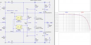
You appear to be correct about increasing Ropto1 (and Rcs) causing a reduction in sensitivity. Below is a AC analysis, used to display the current gain thru the servo to the bias spreader and back thru the FETs. The feedback loops are broken between the Vd+ and Vd- nodes and the servo input circuit. The current sources I1 and I2 provide the AC stimulus, and I(R1) and I(R22) are the resulting currents thru the output FETs. With the resistor values shown, the current gain from input to output is about +3dB.
Attachments
Don´t stop Ian, very interesting dialog and Lynn needs a good partner understanding his explorations.....
:--))
Thank you, I will keep plugging away. Just didn't want to interrupt or monopolise the thread.
You appear to be correct about increasing Ropto1 (and Rcs) causing a reduction in sensitivity. Below is a AC analysis, used to display the current gain thru the servo to the bias spreader and back thru the FETs. The feedback loops are broken between the Vd+ and Vd- nodes and the servo input circuit. The current sources I1 and I2 provide the AC stimulus, and I(R1) and I(R22) are the resulting currents thru the output FETs. With the resistor values shown, the current gain from input to output is about +3dB.
You have confirmed my worry, 3dB is not a lot of gain. I have a variation in mind that I hope will address this aspect. I'll draw it up when I have a spare moment and post it here.
Anyone else care to offer their ideas on this or solving the DC response challenge?
grrrrr! How frustrating..I seem to have come to this thread way too late. I've read it through a couple of times and around about January 2017 I had loads of questions.....and my bloody time machine is oook'd...
I was misled by the title of thread in November 2016 so didn't bother looking.
Have any of you kind chaps, Lynn, Pico, Gerd etc got any reasonable ixys spice models you might share, particularly 40p50p and 48n60p
in anticipation
Ed
I was misled by the title of thread in November 2016 so didn't bother looking.
Have any of you kind chaps, Lynn, Pico, Gerd etc got any reasonable ixys spice models you might share, particularly 40p50p and 48n60p
in anticipation
Ed
This is turning out to be a bigger challenge than I had first thought.
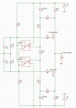
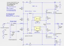
The attached circuit shows the variation of Lynn's circuit that I had envisaged but unfortunately it turns out to be not much better. A word or two of explanation. In order to avoid the bias being reduced when the output stage goes into class B, the purpose of the diodes is to clamp the voltage driving each opto LED at a value of 2 x output bias current.
This works up to a point but it turns out that there is a more fundamental issue with the dual opto circuit. The opto's are being operated at very low currents and the LED current effectively turns off below a certain voltage. This occurs when the output stage current sensed by R15 and R16 approaches zero. The optos are also very non-linear in this region and hence the increase in current from one opto is insufficient to counter the decrease in the other. This leads to the bias voltage falling when a signal is present. In effect this condition is a bit like operating a conventional amplifier output stage in class AB.
Apologies if the above explanation is a little wordy and not very clear.
I'm not sure how to solve this particular behaviour but I have some ideas that I will try out and post my findings.
Attachments
Parallel Opto Bias revisit with Zener SUCCESS?
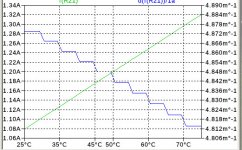
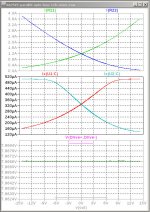
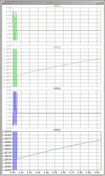
I think I have figured out how to improve the parallel opto servo feedback level from a few dB to 26dB and obtain very good bias stability to frequency, wattage, rail voltage and temperature. I add Zener diodes in the non-zener (0.7V) direction to the opto LED circuits. I also have increased the bias current to 1.2A in order to obtain 25W 4R class-A. The plots from left to right are:
I think I have figured out how to improve the parallel opto servo feedback level from a few dB to 26dB and obtain very good bias stability to frequency, wattage, rail voltage and temperature. I add Zener diodes in the non-zener (0.7V) direction to the opto LED circuits. I also have increased the bias current to 1.2A in order to obtain 25W 4R class-A. The plots from left to right are:
- 25W into 4R at 20Hz, 100Hz, 1kHz, 10kHz
- 1kHz into 4R at 1W, 5W, 25W
- Bias vs Rail Voltage (Vpwr)
- Bias vs Temperature
Attachments
-
 XA25V2-parallel-opto-bias-1xb-zener-bias-vs-TEMP.jpg67.2 KB · Views: 113
 -
 XA25V2-parallel-opto-bias-1xb-zener-bias-vs-Vpwr.jpg66 KB · Views: 96
 -
 XA25V2-parallel-opto-bias-1xb-zener-1kHz-4R-1W-5W-25W.jpg141.6 KB · Views: 304
 -
 XA25V2-parallel-opto-bias-1xb-zener-25W-4R-20Hz-100Hz-1kHz-10kHz.jpg158.4 KB · Views: 360
 -
 XA25V2-parallel-opto-bias-1xb-zener.asc.jpg141.6 KB · Views: 366
Hats off to you Lynn, this really is a great improvement for the cost of just a couple of diodes! It even works well at higher power levels. How did you come up with this idea?
Some questions:
1. Why zener diodes and why 9.1v? Standard diodes would appear to work just as well.
2. Are the values of Ropto1 significant and if so, how to calculate the optimum value?
Now we just need to arrange for the circuit to work DC coupled, i.e. response maintained down to DC")
Some questions:
1. Why zener diodes and why 9.1v? Standard diodes would appear to work just as well.
2. Are the values of Ropto1 significant and if so, how to calculate the optimum value?
Now we just need to arrange for the circuit to work DC coupled, i.e. response maintained down to DC
Lowering he value of the Ropto1 resistor increases the servo feedback, but without the diode that requires a decrease of Rcs. Lowering the value of Rcs increases the sensitivity to rail voltage changes. Adding the diodes provides the way to get more feedback and also keep the rail voltage sensitivity low.Hats off to you Lynn, this really is a great improvement for the cost of just a couple of diodes! It even works well at higher power levels. How did you come up with this idea?
Some questions:
1. Why zener diodes and why 9.1v? Standard diodes would appear to work just as well.
2. Are the values of Ropto1 significant and if so, how to calculate the optimum value?
Now we just need to arrange for the circuit to work DC coupled, i.e. response maintained down to DC
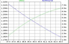
The key appears to be choosing a diode with the right voltage drop at the operating current. Ordinary diodes appeared to have too much voltage drop. I tried using a Schottky diode and then I tried a zener in the forward direction. I used a 9.1V zener because I already had a SPICE model for it. The diode temperature coefficient might also be important also.
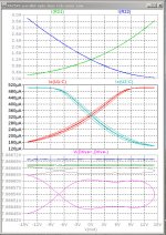
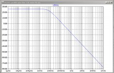
Bot the amplifier input and the bias servo AC response remain flat down to DC....
Now we just need to arrange for the circuit to work DC coupled, i.e. response maintained down to DC
The first plot is the AC response for the amplifier input. The second plot is the AC response for the bias servo. As you can see both are flat down to DC.
The amplifier being DC coupled will amplify and DC offset on the input by the closed-loop gain of the amplifier. Thus a .1V input offset will result in a 1V output offset with this amplifier.
Attachments
since ZM knows Station , can you just give me info in layman terms ...........
simple test :
5mS of silence , 1S of full throttle (say 40Vpp/8R) , 1S of silence ;
what's difference (sag) of Iq immediately after 1S burst , and what is time to Iq recover to initial value
TIA
FYI : I abandoned PL solutions , both with 0R47 and newer one with (supposedly) 167mR ; I believe we got it , in various ways , how Papa did it .... so , why not trying it in different way
also , after extensive (read- hysterical and depression inducing) simulations , I abandoned ACS723 solution , and revert to cascoded current mirror approach (0R1 sense in rails ; maybe even lower is possible ..... didn't tried) .....idea for which I got here , where else
problem with ACS723 is that load can't be lower than 4K7 , and even with buffering , I simply can't get adequate transfer characteristic to tame/compete with insane xconductance of pucks , without resorting to gain element after ACS ......
while cascoded current mirror based circuit is having simply ridiculous sim results (read- minuscule changes) , regarding Vcc step and Temp step behavior , and above explained burst test is resulting in 50mA Iq sag and around 300mS recovery time
all this ...... just to say that I'm reading it all , just don't have really anything useful to add
since ZM knows Station , can you just give me info in layman terms ...........
simple test :
5mS of silence , 1S of full throttle (say 40Vpp/8R) , 1S of silence ;
what's difference (sag) of Iq immediately after 1S burst , and what is time to Iq recover to initial value
...
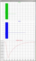
As requested. 100Hz 25W into 8R. The bias change in the 1sec burst is about 8mA and in the 1sec recovery it is about 5mA. Apparently 1sec isn't long enough to fully recover.
Attachments
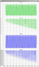
I looked closer at the plots and have corrections to my numbers. The initial bias is 1.200A for each FET. After the 1sec burst the sag is -15mA. After the 1sec recovery the sag is -10mA. After 2.67secs of recovery the sag is -5mA.
What effect will a sag of that magnitude have on the sound of the amplifier?
What effect will a sag of that magnitude have on the sound of the amplifier?
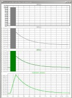
Here is a better presentation of the bias current sag and recovery. The bottom plot is the gate-to-gate voltage difference, which determines the bias current. The initial silence is 0.5sec, burst 1sec, and recovery 10sec.
Attachments
Bot the amplifier input and the bias servo AC response remain flat down to DC.
The first plot is the AC response for the amplifier input. The second plot is the AC response for the bias servo. As you can see both are flat down to DC.
The amplifier being DC coupled will amplify and DC offset on the input by the closed-loop gain of the amplifier. Thus a .1V input offset will result in a 1V output offset with this amplifier.
Sorry, I wasn't sufficiently clear. I meant the output stage as shown does not have a response down to DC. The capacitors C3 and C4 become ineffective and the resistors R14, R12 and R15, R13 act as potential dividers so that there will be some attenuation at DC. All a bit theoretical perhaps but a real effect surely?
- Home
- Amplifiers
- Pass Labs
- F4 Beast Builders