You are correct. The datasheet figure got "high accuracy current source" show a 1634-1.25V Zener diode.LT , I believe connection is in 3092 datasheet
edit: p.18
This may be way too naive, but how about just an LND150 with suitable source resistor for the 0.5mA CCS? Looks to me like the device has nearly a zero temperature coefficient at around 0.5mA. Perhaps it isn't "precise" enough? I see that the bias varies with the CCS current, so precision would be preferred.
Aside from that, has anyone tried using multiple optos like in this circuit by Elvee?
Aside from that, has anyone tried using multiple optos like in this circuit by Elvee?
Last edited:
Yes,Lynn,that is correct.The Pr BJT circuit has the appearance of a current mirror, but I do not think that really is a current mirror. In the first of the circuits shown in post #1026, Q10 is just a common-base amplifier circuit. Q12 establishes the base voltage of Q10 and Q12 being defined by R30*.5mA (CCS current) and Vbe(Q12) which is temperature dependent. The Vbe temperature coefficients of Q10 and Q12 (mostly) cancel.
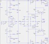
I like to add, that the 220µF capacitors are charged by Q10 and Q9 and discharged by R27 and R28 (pos and neg side independendly). Therefore the value of R27 and R28 only depends from the time constant they form together with the 220µF caps.
R42 und R48 define the gain of the stages.
The bias for the output MOSFETs can be set by changing the values of R30 and R10.
A little bit more explanation:
The chosen constant current source in the appended file is not a simple one but compensates the influence of changes in the power supply voltage.
The common part - thermal stability:
The two LEDs are said to have nearly the same thermal coefficient as the bipolar transistors, so two of them in parallel with Q3 and Q4 should deliver a thermally constant current in both collectors. Noise is suppresed by the 100µF capacitor. To make their oparating current less dependant from the power supply stability, a zener diode stabilizes the voltage over R4 and R5 which in return stabilzes the current through the LEDs.
2 special features - compensation of power supply influence:
R8 and R9 compensate the influence of the changes in the power supply voltage to the bias current of the power MOSFETs I(R100mpos). In the graph I(R100mpos) is constant for R8=R9=820k. But if these resitors are left out (R8=R9=1000G=1TeraOhm), noise signals in the power supply are reflected in the bias.
R14 ist used to trim the output offset to zero. And R13 compensates the influences of the power supply voltage to the offset, as shom in the graph: Vout is constant, with Roffs=0.1 (Roffs in this simulation is used like a switch).
The bonus - D4 and D5:
The diodes protect the bipolar transistors,when the current through the 100mOhm resistors rises above about 50A. In that case Ube can become >5V, which exceeds the limit of typical small transistors. The diodes limit the voltage to 0,7V.
Attachments
Last edited:
Pr: Thank you for the good explanation. Have you actually bench tested this circuit.
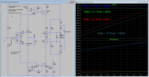
I am interested in how well the LT3092 might perform in comparison, since it replaces 13 parts by 2 parts. ZM suggested using the LT1634-1.25 precision voltage reference with the LT3092. That might be useful if absolute current accuracy was required, but I do not know if it provides any other benefit.
I am interested in how well the LT3092 might perform in comparison, since it replaces 13 parts by 2 parts. ZM suggested using the LT1634-1.25 precision voltage reference with the LT3092. That might be useful if absolute current accuracy was required, but I do not know if it provides any other benefit.
No, only simulation.... I am not retired, I have to go to work, so not much time left...
In my personal opinion absolute current accuracy seems to be less important than suppresion of noise signals from the power supply. In my amp temperature between winter and summer is only about 15k, so I do not expect much change in bias. I could imagine that a precision current source is a litte over the top here. But we are DIYers and we like it over the top... (me dreaming of a bridged amp with 3 IXYS in parallel on each half and side, so 12 in total per channel, and that is over the top )
)
Why don't give both variants a try? Doesn't cost much...
In my personal opinion absolute current accuracy seems to be less important than suppresion of noise signals from the power supply. In my amp temperature between winter and summer is only about 15k, so I do not expect much change in bias. I could imagine that a precision current source is a litte over the top here. But we are DIYers and we like it over the top... (me dreaming of a bridged amp with 3 IXYS in parallel on each half and side, so 12 in total per channel, and that is over the top
)Why don't give both variants a try? Doesn't cost much...
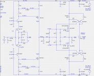
Here is a (nearly) complete amplifier with the BJT servo in the OS and a FE with DC degeneration of the J313/K2013 FETS and no servo. The JFET sources are driven in the manner of the F5, with independent feedback networks for each source pin. The parameter values have not undergone final tuning, but so far the performance looks quite good.
Attachments
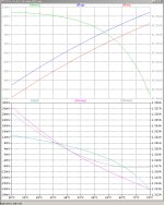
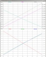
My previous circuit had leftover resistors from OS gates to rails that introduced PSRR issues. Here is a revised circuit that is more like that from Pr that has good temperature and rail voltage insensitivity. The plots below are FE and OS parameters vs. rail voltage.
Attachments
Hello Brothers
No idea what your goals are here, but if you like parts minimization go back and simplify the front end (get rid of the caps and source resistors) and try 2sj79 2sk216.
I decided to give it a go and was happy with the result.
I biased them at 60mA.
Hello PicoDumbs
So no themal runaway with the 79/216? What kind of heatsinks for them?
And you took the "normal" TL circuit for the OS?
Hello PicoDumbs
So no themal runaway with the 79/216? What kind of heatsinks for them?
And you took the "normal" TL circuit for the OS?
No thermal drift on the 79/216.
Output I stayed with TL431 circuit with thermistor.
I will send link for heatsinks.
My initial hesitation was that we might not get adequate open loop gain but that doesn't seem to be a problem after all.
Last edited:
Thanks for the link needtubes, I will Spice things a bit!
as far as I know Lynn tried a long time multiple optos.
This RA-T2X-51E Ohmite | Fans, Thermal Management | DigiKey
Or this RA-T2X-38E Ohmite | Fans, Thermal Management | DigiKey
51mm or 38mm tall whichever one you have room for.
Or this RA-T2X-38E Ohmite | Fans, Thermal Management | DigiKey
51mm or 38mm tall whichever one you have room for.
Spice Models
Would you mind making these available more generally?
Thanks.
I made some 79/216 models if you want them
Would you mind making these available more generally?
Thanks.
They're just a rough first draft.
Vgs threshold, and transconductance curves are accurate, but other parameters may need changing.
Good enough to get a feel for how they might perform, but I might need to make some changes, so not ready to post publicly.
I can send you them via pm if you want them
Vgs threshold, and transconductance curves are accurate, but other parameters may need changing.
Good enough to get a feel for how they might perform, but I might need to make some changes, so not ready to post publicly.
I can send you them via pm if you want them
- Home
- Amplifiers
- Pass Labs
- F4 Beast Builders