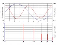
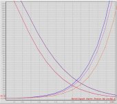
Here are those curves, taken from a BAF talk a couple years ago.
They were taken from this amp or its brothers.
I enjoyed experimenting with DEF Amp; thanks to Mr. Pass for his generous donation of two SJDP120R085 [scarce].
The Distortion Waveform of the DEF Amp is very low, and is second harmonic [H2] negative phase [H2np]. What's causing this asymmetry?
My following explanation of [H2np]; by using this graph is the same as or reiterates that of Mr. Pass in his article entitled H2 Harmonic Generator.
1. Let the amplitude of the Fundamental [Fun] equal 2 Volts peak to peak. Thus, the positive going peak is [1 V], and the negative going valley is [-1 V].
2. Let the amplitude of [H2] equal 0.2 Volts peak to peak. Thus its positive peak is [+0.1 V], and the depth of its valley is [-0.1 V].
3. The above voltages of [Fun] and H2] are numbers which add to each other or one subtracts from the other depending on the time-coincidence of the peaks or valleys of [ Fun] and [H2].
4. Using wording like that written by Mr. Pass:
4a. when the peak of [Fun] is [+1 V], the time-coincident valley of [H2] is [-0.1 V]. This voltage of H2 subtracts from that of [ Fun] to give a net equal to [+0.9 V].
4b. When the upcoming valley of [Fun] hits bottom at [ -1 V], the time-coincident valley of [H2] hits bottom too at [- 0.1 V]. The voltage of [Fun] and [H2 ] add to each other to give a resultant valley of depth equal [-1.1 V].
5. The resultant new signal is now called [H2np]. [Fun] and [H2np] signals are in-phase. The peak of [H2np] sits at [+0.9 V], and its valley sits at [-1.1 Vp].
6. Next I compare these two signals [Fun] and [H2np] as follows:
6a. Normalize the value of the valley of [H2np] which is [-1.1 V] or make it equal to [-1 V] like that of the valley of [Fun] which is [- 1 V]
6b. This allows one to calculate a new value for the peak of [H2np] which is [ + 0.9 V divided by 1.1 V ] equal to [+0.82 V]
7. Mentally superimpose the waveform of [H2np] atop [Fun]. You are looking or visualizing the answer of "What is H2np"? The positive peak of [Fun] shrank to 82% its original value while holding constant [ at -1 V] the valley depth of [ Fun] and [H2np].
8. The two electrical signal are converted to pressure wave which reach the ear drum. The two signals will sound different; because of the resultant two different inward displacements of the eardrum.
9. My brain will then signal which of the two pressure waves it likes best!
Best
Anton
DEF experiment
Attached is a picture of a DEF pair; IXTH16N50D2 and a fake eBay 2SJ618. Surprisingly, the 2SJ618 meets Toshiba's datasheet specs for Vth and gain. The cutouts and holes of the device package do not match the datasheet drawing.
Voltage rails were set at + / - 2V. Current is 765mA. Vgs is shown on the multimeter at ~ 80mV. The gates are floating.
Temp of the IXTH part is ~ 55 C and the 2SJ part is around 45 C.
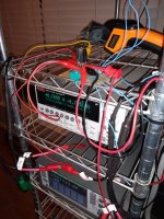
Next will be to mount the devices on a heatsink, move them to a rack with a power supply and DMM and try the pair at higher rail voltages. It is fun to see how the devices behave in this configuration.
I will fully measure the gain and Vgs of each device and report back here.
Attached is a picture of a DEF pair; IXTH16N50D2 and a fake eBay 2SJ618. Surprisingly, the 2SJ618 meets Toshiba's datasheet specs for Vth and gain. The cutouts and holes of the device package do not match the datasheet drawing.
Voltage rails were set at + / - 2V. Current is 765mA. Vgs is shown on the multimeter at ~ 80mV. The gates are floating.
Temp of the IXTH part is ~ 55 C and the 2SJ part is around 45 C.
Next will be to mount the devices on a heatsink, move them to a rack with a power supply and DMM and try the pair at higher rail voltages. It is fun to see how the devices behave in this configuration.
I will fully measure the gain and Vgs of each device and report back here.
Attachments
Last edited:
I found an incorrect connection and I added a resistor from gate to power supplies common.
Changed rails to + / - 4V.
Vgs is now -1.76V, current is 670 mA cold. Need to mount these to a heatsink next. Vgs makes more sense now.
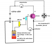
Hello woofertester. Please show the schematic of the prototype that you are experimenting with. Thanks
Best
Anton
Hello Anton
It is Nelon's original post of two devices arranged as a push-pull follower pair. N-channel depletion on top. P-channel enhancement on bottom.
It is Nelon's original post of two devices arranged as a push-pull follower pair. N-channel depletion on top. P-channel enhancement on bottom.
Hello woofertester. Please show the schematic of the prototype that you are experimenting with. Thanks
Best
Anton
Hello Anton
It is Nelon's original post of two devices arranged as a push-pull follower pair. N-channel depletion on top. P-channel enhancement on bottom.
Hello woofertester. It is important as you wrote to put DEF on a heatsink. May wish to consider adding a 1 Ohm/5W degeneration resistor per device to further protect it from overdissipation. This will allow you to slowly increase the PSU rails to a magnitude higher than +/-4 V so as to listen to the resultant DEF. My suggested degeneration resistors can thereafter be lowered methodically while noting the dissipation of DEF and finally removed.
Best
Anton
Hello Anton
The idea was to check Vgs at temperature at bias current for normal class A operation. I was able to get the temperature I was looking for at class A current without a heat sink by keeping Vds low. Just the first step. Heatsink mounting is next.
I have again played with the DEF. The three UJN1208K now have three better matched IRFP9240 @ 24V/1.3A. These are the pairs:
n.1 Vgs(UJN)= -4.122V, Vgs(IRFP)= -4.102V
n.2 Vgs(UJN)= -4.261V, Vgs(IRFP)= -4.217V
n.3 Vgs(UJN)= -4.051V, Vgs(IRFP)= -4.075V
The bias voltage is the average between the two voltages. I used the first pair. The circuit has only three resistors, a Zener and a capacitor at the input. There is no capacitor at the output. I stressed the circuit in all possible ways. Current, bias voltage and output offset have always been stable. Cold < 20mV, < -7mV after 60 minutes of music. The current is a little higher ( 1.36A ) because the Vgs of the UJN is more negative than the IRPEF.
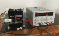
The first photo: THD= -62.5dB @ 1W/8R. The second photo: THD= -45.6dB @ 14.5W/8R ( +Peter Millet's Soundcard Interface ). The third: the amp. The pcb connected to the gates is the separate power supply for the bias. willnot be easy to build the chassis that use my heatsink. Not to mention the power supply.
n.1 Vgs(UJN)= -4.122V, Vgs(IRFP)= -4.102V
n.2 Vgs(UJN)= -4.261V, Vgs(IRFP)= -4.217V
n.3 Vgs(UJN)= -4.051V, Vgs(IRFP)= -4.075V
The bias voltage is the average between the two voltages. I used the first pair. The circuit has only three resistors, a Zener and a capacitor at the input. There is no capacitor at the output. I stressed the circuit in all possible ways. Current, bias voltage and output offset have always been stable. Cold < 20mV, < -7mV after 60 minutes of music. The current is a little higher ( 1.36A ) because the Vgs of the UJN is more negative than the IRPEF.
The first photo: THD= -62.5dB @ 1W/8R. The second photo: THD= -45.6dB @ 14.5W/8R ( +Peter Millet's Soundcard Interface ). The third: the amp. The pcb connected to the gates is the separate power supply for the bias. willnot be easy to build the chassis that use my heatsink. Not to mention the power supply.
Attachments
Mouser refers to UJ3N120070K3S as a similar product. There is also the UJ3N065080K3S which costs a little less. Compared to UJN1208K both have a tranfer characteristics shifted to more negative values of Vgs. They should be tried. In the next order I will to insert the second SIC.
There’s also a new product, UJ3N120065K3S, with a typ. Vgs of -6.6V (defined @ Id of 35mA), which is right in the middle between UJN1208K’s -7V and UJN1205K’s -6V (both @ Id of 70mA though). Mouser expects to have some stock in a couple of weeks...
Last edited:
Definitely! ") But those -6.6V are @ 35mA - it should be closer to -4V @ ~1A, as shown by claudio52's measurements of UJN1208K. And -4V @ ~1A should be much easier to achieve with UJ3N120065K3S than with UJ3N120070K3S or UJ3N065080K3S that have a typ. Vgs of -11.5V (@ 35 and 20mA, respectively).
But those -6.6V are @ 35mA - it should be closer to -4V @ ~1A, as shown by claudio52's measurements of UJN1208K. And -4V @ ~1A should be much easier to achieve with UJ3N120065K3S than with UJ3N120070K3S or UJ3N065080K3S that have a typ. Vgs of -11.5V (@ 35 and 20mA, respectively).
But those -6.6V are @ 35mA - it should be closer to -4V @ ~1A, as shown by claudio52's measurements of UJN1208K. And -4V @ ~1A should be much easier to achieve with UJ3N120065K3S than with UJ3N120070K3S or UJ3N065080K3S that have a typ. Vgs of -11.5V (@ 35 and 20mA, respectively).Level shift Vgs of PMOS
Hi Zen Mod,
Fully agree. I experimented with level-shifting [Vgs] of PMOS [e.g from -3.7V] to more negative values. With 1 PNP it added [-0.6 V]or its Darlington which added [-1.2V] so as to ~match the high-valued Vgs [+ 5V ] of NFET. Worked.
Please see posts#83 and 116 for examples which showed another method, and some data.
Best
Anton
though, for ultrasimple DEF, 4V figure is a must
Hi Zen Mod,
Fully agree. I experimented with level-shifting [Vgs] of PMOS [e.g from -3.7V] to more negative values. With 1 PNP it added [-0.6 V]or its Darlington which added [-1.2V] so as to ~match the high-valued Vgs [+ 5V ] of NFET. Worked.
Please see posts#83 and 116 for examples which showed another method, and some data.
Best
Anton
Last edited:
Just tested 2 pieces of IXYS IXTH6N50D2 @24V with target Id of 1.3A. Device was mounted to heatsink and monitored as it came up to temperature.
Not meant to be generalization for all samples but in my case, the Vgs is too low to be easily used in a DEF amp.
IXTH6N50D2
Sample 1 - Vgs = -1.85V, Id = 1.305A (approx 40C)
Sample 2 - Vgs = -1.90V, Id = 1.296A (approx 40C)
Datasheet values for 25V @ 250uA gives range between -2.5V and -4.5V for reference.
The only P-channel mosfets that I have that are remotely close are a small number of 2SJ201(Y) so I re-measured the 2 lowest Vgs of them for -24V and 1.3A
2SJ201(Y)
Sample 1 - Vgs = -2.035V, Id = 1.33A
Sample 2 - Vgs = -2.031V, Id = 1.30A
Next stop is a visit to the protoboard but I have higher hopes for a few United UJ3N120065K3S on order where I'm hoping to find some matches for IRFP9240 (Harris) or Fairchild (around 5.5V range) where the population of parts is much larger compared to 2SJ201
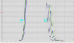
Attached Locky_Z (room temperature) traces for the IXYS and Toshibas to show just how different these numbers are from my Idss test set up numbers.
Not meant to be generalization for all samples but in my case, the Vgs is too low to be easily used in a DEF amp.
IXTH6N50D2
Sample 1 - Vgs = -1.85V, Id = 1.305A (approx 40C)
Sample 2 - Vgs = -1.90V, Id = 1.296A (approx 40C)
Datasheet values for 25V @ 250uA gives range between -2.5V and -4.5V for reference.
The only P-channel mosfets that I have that are remotely close are a small number of 2SJ201(Y) so I re-measured the 2 lowest Vgs of them for -24V and 1.3A
2SJ201(Y)
Sample 1 - Vgs = -2.035V, Id = 1.33A
Sample 2 - Vgs = -2.031V, Id = 1.30A
Next stop is a visit to the protoboard but I have higher hopes for a few United UJ3N120065K3S on order where I'm hoping to find some matches for IRFP9240 (Harris) or Fairchild (around 5.5V range) where the population of parts is much larger compared to 2SJ201
Attached Locky_Z (room temperature) traces for the IXYS and Toshibas to show just how different these numbers are from my Idss test set up numbers.
Attachments
Not all UJN parts are alike
Update: I received the UJ3N120065K3S today and measured 1 in the test harness:
Id: 1.305A @ Vgs: 6.35V positive tempco
This was much higher than I was hoping for based on the feedback from the UJN1208K which seemed to measure a full 3V below the datasheet (7V) number.
Not a total loss yet however because I remember that the Fairchild mosfets used in the F5 were a full 1V higher Vgs than the IRF counterparts so I took out a random sample and:
Id: 1.312A @ Vgs: 5.65V
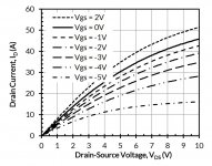
A full 0.7V difference but I thought I would take a look at how bad this could be and tried to calculate the potential extra bias. Thankfully the depletion part Vgs is higher and can be tamed a bit with degeneration. gfs for the Fairchild FQA12P20C is 6.6 and there is no gfs number for the United part so I went to the Vds/Ids graph which was present. If the calculation is correct then at -5V Vgs, you get roughly 15A change over a 7V delta or roughly 2.14 transconductance.
Plugging this into Papa's formula you get:
delta I = (6.35-5.65)*(1/2.14 + 1/6.6) = 0.433
So assuming no degeneration, I might be looking at 1.3A + 0.433 = 1.73A @24V ... a bit on the high side but still within my definition of "it should work" ...
to be continued ...
Attached Locky_Z curves of the UJN parts and Fairchild P-channel mosfets. Again, the Locky_Z curves are much more conservative compared to what I measure on heatsink so imagine the left side curves sliding over a bit to the right (-5.65V @1300mA) and the right side (N-sic) curves moving to the left (-6.35V @1300mA). Apply an appropriate amount of N-sic degeneration and you can find an intersection somewhere in the desired range of 1300-1700mA as available heatsinking will allow. At least that's what I understand of the theory ...
Cheers,
Stephen
Update: I received the UJ3N120065K3S today and measured 1 in the test harness:
Id: 1.305A @ Vgs: 6.35V positive tempco
This was much higher than I was hoping for based on the feedback from the UJN1208K which seemed to measure a full 3V below the datasheet (7V) number.
Not a total loss yet however because I remember that the Fairchild mosfets used in the F5 were a full 1V higher Vgs than the IRF counterparts so I took out a random sample and:
Id: 1.312A @ Vgs: 5.65V
A full 0.7V difference but I thought I would take a look at how bad this could be and tried to calculate the potential extra bias. Thankfully the depletion part Vgs is higher and can be tamed a bit with degeneration. gfs for the Fairchild FQA12P20C is 6.6 and there is no gfs number for the United part so I went to the Vds/Ids graph which was present. If the calculation is correct then at -5V Vgs, you get roughly 15A change over a 7V delta or roughly 2.14 transconductance.
Plugging this into Papa's formula you get:
delta I = (6.35-5.65)*(1/2.14 + 1/6.6) = 0.433
So assuming no degeneration, I might be looking at 1.3A + 0.433 = 1.73A @24V ... a bit on the high side but still within my definition of "it should work" ...
to be continued ...
Attached Locky_Z curves of the UJN parts and Fairchild P-channel mosfets. Again, the Locky_Z curves are much more conservative compared to what I measure on heatsink so imagine the left side curves sliding over a bit to the right (-5.65V @1300mA) and the right side (N-sic) curves moving to the left (-6.35V @1300mA). Apply an appropriate amount of N-sic degeneration and you can find an intersection somewhere in the desired range of 1300-1700mA as available heatsinking will allow. At least that's what I understand of the theory ...
Cheers,
Stephen
Attachments
- Home
- Amplifiers
- Pass Labs
- DEF Amp