Experimenting with DEF
I have two SJDP120R085 [R085] FETs. The previous posts pertained to one which gave me an "ideal" DEF; like its schematic shown in the first post. This depletion FET has a 0 gate current , and a Vgs = -3.65 V; which matched that of the partner P-MOSFET. This "match" status means that this joint Vgs = -3.65 V, gave equal +/- drain currents [Id] at equal +/- drain-source voltages [Vds]. This enabled the joint sources of the FETs in DEF to sit at ~0 Vdc for direct coupling to the loudspeaker [no output cap needed].
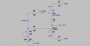
The second R085 has a gate current of ~11 mA [may vary], and a Vgs = -5.4 V. This depletion FET is thus mismatched with the same P-MOSFET which has a Vgs = -3.65 V. The revised DEF schematic which rendered this R085 useable in a power amp was shown by Mr. Pass in his BAF 2016 part 2 presentation at time = 24 minutes. It shows a DEF configuration which uses one degeneration resistor joining the two source ports of the FETs.
The left schematic was used to assemble this revised DEF. It accomplishes the following important requirements:
1. The gate current of R085 [11 mA] was dumped in the -12 V low power rail through a variable power resistor made of two 500 Ohm pots [wirewound].
2. This variable power resistor was then ideally used to generate the joint Vgs in this DEF which gave a 0 Vdc output offset.
3. Several degeneration power resistors [4, 2, 1, Ohms] were tried to join the sources of the FETs. Resistor = 2 Ohms was used as it gave a stable DEF which has a respectable Id = +/-0.8A at +/- 10 Vds. Should one need a lower Id at the same +/- 10 Vds, then a higher valued degeneration resistor was demonstrated; [3 Ohms gave +/-0.6 A].
4. The degen resistor and adjusting the values of two 500 Ohm pots, an output voltage offset of <50 mV was obtained. The measured value of this resistor at the joint gates was ~780 Ohms.
5. Think of this 2 Ohm degen power resistor as an integral part of this R085; though it is external to it. Its new source port is Vout.
6. The voltage drop across the 2 Ohm degen resistor = 1.6 V. Add it to the joint Vgs = 3.75 to get a value of 5.4 V. This is the value measured between the gate of R085 and its source.
How did it sound?. Way better and highly refined after adding a 3,300 uF [decouple cap] across the 2 Ohm degen resistor as shown in the right schematic.
This R085 is highly useable.
I have two SJDP120R085 [R085] FETs. The previous posts pertained to one which gave me an "ideal" DEF; like its schematic shown in the first post. This depletion FET has a 0 gate current , and a Vgs = -3.65 V; which matched that of the partner P-MOSFET. This "match" status means that this joint Vgs = -3.65 V, gave equal +/- drain currents [Id] at equal +/- drain-source voltages [Vds]. This enabled the joint sources of the FETs in DEF to sit at ~0 Vdc for direct coupling to the loudspeaker [no output cap needed].
The second R085 has a gate current of ~11 mA [may vary], and a Vgs = -5.4 V. This depletion FET is thus mismatched with the same P-MOSFET which has a Vgs = -3.65 V. The revised DEF schematic which rendered this R085 useable in a power amp was shown by Mr. Pass in his BAF 2016 part 2 presentation at time = 24 minutes. It shows a DEF configuration which uses one degeneration resistor joining the two source ports of the FETs.
The left schematic was used to assemble this revised DEF. It accomplishes the following important requirements:
1. The gate current of R085 [11 mA] was dumped in the -12 V low power rail through a variable power resistor made of two 500 Ohm pots [wirewound].
2. This variable power resistor was then ideally used to generate the joint Vgs in this DEF which gave a 0 Vdc output offset.
3. Several degeneration power resistors [4, 2, 1, Ohms] were tried to join the sources of the FETs. Resistor = 2 Ohms was used as it gave a stable DEF which has a respectable Id = +/-0.8A at +/- 10 Vds. Should one need a lower Id at the same +/- 10 Vds, then a higher valued degeneration resistor was demonstrated; [3 Ohms gave +/-0.6 A].
4. The degen resistor and adjusting the values of two 500 Ohm pots, an output voltage offset of <50 mV was obtained. The measured value of this resistor at the joint gates was ~780 Ohms.
5. Think of this 2 Ohm degen power resistor as an integral part of this R085; though it is external to it. Its new source port is Vout.
6. The voltage drop across the 2 Ohm degen resistor = 1.6 V. Add it to the joint Vgs = 3.75 to get a value of 5.4 V. This is the value measured between the gate of R085 and its source.
How did it sound?. Way better and highly refined after adding a 3,300 uF [decouple cap] across the 2 Ohm degen resistor as shown in the right schematic.
This R085 is highly useable.
Attachments
which has some interesting
characteristics, not the least of which is low temperature drift which allows
stable undegenerated operation.
I have been intrigued by Nelson Pass DEF-amp, but I don´t have any suitable depletion-mode devices to test it.
I have watched the BAF2016 talk and the idea of using no (or at least very low value) source-resistors seems very promising.
The only solution I have found, except the brute-force massive heatsink and "big ba_ls" (and a couple of spare mosfets), is the Triadtron circuit.


I quickly simulated this pure class A "Triadtron" circuit with the IRFP240 + IRFP9240. The circuit is not as simple and nice as Nelson Pass DEF-amp, but it is one way to circumvent having to use the source-resistors for a stable bias and quiescent current.
The simulated performance is quite good. I have not built it yet, but I am playing with the circuit in LTSpice and I hope I can build a test-channel soon.
Cheers,
Johannes
I have been intrigued by Nelson Pass DEF-amp, but I don´t have any suitable depletion-mode devices to test it.
I have watched the BAF2016 talk and the idea of using no (or at least very low value) source-resistors seems very promising.
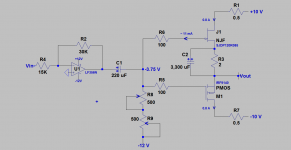
Hello Johannes. Thank you for the interesting schematic. Clearly, my use of a 2 Ohm degen resistor and a large decoupling cap across it works [previous post]; but is not practically attractive. I have been mulling the attached DEF schematic as a potential alternative solution for the situation of a gross Vgs mismatch between the FETs; in this schematic example a value of 1.2 Volts.
Suppose the NJF [e.g R085 or other] has a Vgs = -5.0 V, and no gate current. Its companion P-MOSFET [IRF9140] has a Vgs = -3.7 V. This -1.2 V difference or gap is ~closed with a PJF driving the R085 as shown. This PJF is assumed to have a Vgs of +1.2 V. Thus it lifts the Vgs of R085 to a more positive value; which ends at ~ -3.8 V. A small degen resistor [~0.1 Ohm] between the sources of the power FETs is therafter used to fully match'em.
Since my second SJDP120R085 has a gate current [~11 mA] and a gross Vgs mismatch of 1.6V, I'll experiment with LM 337 [negative voltage regulator] as a pseudo power PJF ; because it has +1.25 V between its adjust and output ports. The resultant degen resistor in this alternative DEF is expected to be smaller than 2 Ohms.
The use of LM337 like a depletion FET was suggested by Johannes during the thread of F6.
Attachments
Experimenting with DEF
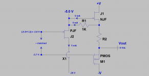
The attached schematic was assembled to make a prototype DEF power amp which is stable, sounds great with no hiss/hum and has a zero DC offset at its power output. Let's examine the schematic from its rightside and moving left:
1. There are no degeneration resistors between the FET sources.
2. Drain current in each FET is ~0.9A.
3. Vds of each FET is 15 V
4. The 0.01 uF capacitor between the gate and the drain of R085 cleared a small amplitude MHz oscillation.
5. The Vgs of R085 [-5.48V] is substantially smaller than that of IRF9140 [-3.71 V]. The FETs are grossly mismatched [delta Vgs = 1.8 V].
6. The LM337 variable negative voltage regulator was used to shift the Vgs of R085 from -5.48 V to -3.71 V so as to effect a "match" between the FETs.
7. LM337 is configured as published in its application to generate a -5.78 V stable output.
8. The resistors [220, 140 and 630 Ohms] support LM337 as a voltage regulator.
9. Normally the resistors [140 +630 = 770 Ohms] are connected to ground. In the schematic [and amp] they are connected to power output which is at zero Volts. This connection allows the fixed output voltage of the regulator to ride with the input or output music signal.
10. I segmented the 770 Ohm resistor [not shown] into 140 Ohms and 630 Ohms so as to generate the voltage level shift to its final value of -3.71 V which goes to the gate of IRF9140.
11. A DC servo is shown. It locks the power output at zero DC Volts, and the pseudo matched Vgs at -3.71V. Without it, the output voltage offset drifts.
12. This particular R085 has a gate current of ~10 mA. LM337 sinks it.
I was tempted early on in these experiments to discard this $50 R085. Clearly, the above showed me that it is fully useable; but with an increase in circuit complexity.
Attachments
I have not found need to compensate these circuits with a cap, but then
you clearly have a defective R085 given the 10 mA Gate current.
Most of these have Gate currents below 20 uA.
Also, I routinely get matches to 0.3V.
Is this really a 50$ part? I didn't think there were any still available.
you clearly have a defective R085 given the 10 mA Gate current.
Most of these have Gate currents below 20 uA.
Also, I routinely get matches to 0.3V.
Is this really a 50$ part? I didn't think there were any still available.
Last edited:
I have not found need to compensate these circuits with a cap, but then
you clearly have a defective R085 given the 10 mA Gate current.
Most of these have Gate currents below 20 uA.
Also, I routinely get matches to 0.3V.
Is this really a 50$ part? I didn't think there were any still available.
I bought two R085 from iMPOWER Systems, Inc [Dr. Mazzola] on Aug. 20 2015 for ~100$. I damaged one [got gate current] while using both in a Class aP application. Then, DIYer Tea Bag also had a stash of R085s; each selling for ~45$.
My good R085 has a performance like you said above. I easily made a low power DEF [with IRF9140] without any problems.
Please mention the expected/measured output impedance of DEF. Thank you.
Please mention the expected/measured output impedance of DEF. Thank you.
You can easily determine that for yourself
You can easily determine that for yourself
Mr. Pass is the one and only who is qualified to declare an accurate value of the output impedance of his DEF. This valuable number determines its subjective sonics, and will be remembered by DIYers as 'the trusted number" for a long time . Really, will you trust my Zo number from the messy prototype I showed in an earlier post? I don't. But; I say that with overall negative feedback [my first post] Zo of DEF is going to be <0 Ohms. Still the soft base I heard with my DEF which had an absent overall negative feedback suggested its Zo maybe >0 Ohms.
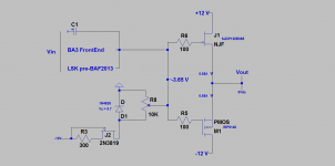
The attached schematic of a low power DEF amp [earlier post] proposes using preamps like BA3 Front End, or LSK pre-BAF2013 to drive its input directly instead of another preamp which requires an output coupling capacitor. The externally imposed or internally generated offset of -3.65 V by the aforementioned preamps at their opposed drains, or collector outputs respectively, will [hopefully] not disturb their parent performance.
Attachments
Last edited:
Let's match the FETs in DEF. Start with SJDP120R085
The variable PSU I am using to experiment with DEF is that of a Radio Shack receiver [STA 2000D]. It is a classical type. The secondary of the iron power transformer is center tapped and goes to a bridge rectifier which is then connected to two 15,000 uF filter caps. I plug the receiver's power cord in the variable socket of a variac. Here is the the turn on process.
1. Adjust variac setting to 15 Vac, and turn its power on.
2. Turn power on to receiver. Got a +/-5 Vdc rail voltage to DEF. I always start at +/-5 Vdc to protect the FETs.
3. The receiver has a feature which discharges its main PSU c/o a relay and power resistors upon turn off.
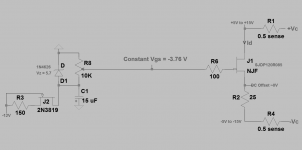
The attached schematic was used to determine the special value of Vgs for SJDP120R085. I also need to declare Id and Vds which are attendant to this Vgs as I'll show below.
1. The left side of the schematic is a stable bias [Vgs] generator. It sits on a protoboard. Constant current [~4 mA] flows from ground through the Zener and through the sink [2N3819] circuit. The 10 K variable resistor is then adjusted for a unique value of Vgs. Turn power on to this bias circuit first.
2. The right side of the schematic shows the test circuit for R085. R085 sits on a heatsink; because it'll dissipate some power.
3. A 25 Ohm/25 W resistor connects the source of R085 to the negative PSU rail; from the Radio Shack receiver.
Power [+/- 5V] was next applied across R085/25 Ohm resistor.
1. The only objective was to adjust the bias voltage Vgs such that the voltage at the source of R085 [reference ground] is equal to 0 Vdc.
2. Fine tune Vds to +5 V, and fine tune Vgs [-3.76 V] such that the source of R085 [output] has a 0 Vdc offset. It was about 20 mV.
3. Finally I need to declare Id; which is equal to ~200 mA by measuring the voltage drop across either 0.5 Ohm sense resistors and multiply it by two.
4. It is important to note that the 25 Ohm power resistor is solely responsible to set Id = 200 mA; from Ohm'Law 5 V/25 Ohms = 200 mA.
5. System is stable. No drift of Id or output DC offset
6. Increased the variac setting such that Vds =10 V. The current Id doubled to ~400 mA [10 V/25 Ohm], and output DC offset ~20 mV or less. Vgs was still at -3.76 V. Stable Id and output offset.
7. Increased variac setting such that Vds =15 V. The current Id was measured at ~600 mA [tripled], and the output DC offset was equal to ~0 V. Vgs still measured at -3.76 V. Stable Id and output voltage offset.
I expect at a Vds = 20 V, and 25 V , that Id will measure at 800 mA and 1 A respestively. Because the earlier measurements of Id versus Vds [5V to 15 V] were directly proportional or linear.
Next post will address the electrical characterestics of IRFP9140 using the identical procedure above.
The variable PSU I am using to experiment with DEF is that of a Radio Shack receiver [STA 2000D]. It is a classical type. The secondary of the iron power transformer is center tapped and goes to a bridge rectifier which is then connected to two 15,000 uF filter caps. I plug the receiver's power cord in the variable socket of a variac. Here is the the turn on process.
1. Adjust variac setting to 15 Vac, and turn its power on.
2. Turn power on to receiver. Got a +/-5 Vdc rail voltage to DEF. I always start at +/-5 Vdc to protect the FETs.
3. The receiver has a feature which discharges its main PSU c/o a relay and power resistors upon turn off.
The attached schematic was used to determine the special value of Vgs for SJDP120R085. I also need to declare Id and Vds which are attendant to this Vgs as I'll show below.
1. The left side of the schematic is a stable bias [Vgs] generator. It sits on a protoboard. Constant current [~4 mA] flows from ground through the Zener and through the sink [2N3819] circuit. The 10 K variable resistor is then adjusted for a unique value of Vgs. Turn power on to this bias circuit first.
2. The right side of the schematic shows the test circuit for R085. R085 sits on a heatsink; because it'll dissipate some power.
3. A 25 Ohm/25 W resistor connects the source of R085 to the negative PSU rail; from the Radio Shack receiver.
Power [+/- 5V] was next applied across R085/25 Ohm resistor.
1. The only objective was to adjust the bias voltage Vgs such that the voltage at the source of R085 [reference ground] is equal to 0 Vdc.
2. Fine tune Vds to +5 V, and fine tune Vgs [-3.76 V] such that the source of R085 [output] has a 0 Vdc offset. It was about 20 mV.
3. Finally I need to declare Id; which is equal to ~200 mA by measuring the voltage drop across either 0.5 Ohm sense resistors and multiply it by two.
4. It is important to note that the 25 Ohm power resistor is solely responsible to set Id = 200 mA; from Ohm'Law 5 V/25 Ohms = 200 mA.
5. System is stable. No drift of Id or output DC offset
6. Increased the variac setting such that Vds =10 V. The current Id doubled to ~400 mA [10 V/25 Ohm], and output DC offset ~20 mV or less. Vgs was still at -3.76 V. Stable Id and output offset.
7. Increased variac setting such that Vds =15 V. The current Id was measured at ~600 mA [tripled], and the output DC offset was equal to ~0 V. Vgs still measured at -3.76 V. Stable Id and output voltage offset.
I expect at a Vds = 20 V, and 25 V , that Id will measure at 800 mA and 1 A respestively. Because the earlier measurements of Id versus Vds [5V to 15 V] were directly proportional or linear.
Next post will address the electrical characterestics of IRFP9140 using the identical procedure above.
Attachments
You have a PM
Hello Mr. Pass. Thank you for your message. I replied to you.
Electrical characteristics of IRFP9140 for DEF with SJDP120R085
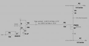
The P-Mosfet IRFP9140 is the companion of SJDP120R085 in my DEF. I used the same procedure/equipment described earlier to determine its relative matching to R085. The attached schematic shows the test circuit. IRFP9140 was attached to a heatsink as it dissipated some power during the test.
1. At a Vds= -5V, Vgs was -3.45V. It gave a zero output DC offset and an Id of 200 mA.
2. For a Vds = -10 V, the DC offset was greater than 100 mV. The 10K bias resistor was adjusted [Vgs ~-3.55 V] to restore a zero DC output offset, and an Id ~400 mA.
3. For a Vds = -15 V, the DC offset was again greater than a 100 mV. The 10 K bias resistor was adjusted to give a Vgs ~ -3.65 V. This Vgs restored an output DC offset to zero V, and an Id ~ 600 mA.
At a Vds of +/- 15V, the Vgs gap or difference between the two FETs was at a minimum of ~ 100 mV from the difference between 3.76 V [R085]of the previous post and 3.65 V of the P-MOS. It maybe possible to further minimize this difference at Vds >+/- 15 V.
Are the FETs matched at a Vds =+/- 15V with this minimum delta Vgs ~100 mV? I'll answer in the next post.
Attachments
On matching FETs in DEF
The FETs in my DEF are Vgs matched to within 0.1V at an Id =0.6A, Vds= +/-15 V, and an output voltage offset equal to zero.
So, the FETs: SJDP120R085 and IRFP9140 were then connected as prescribed by Mr. Pass in post#1 of this thread. Their gates were joined, and so were their sources; but without intervening degeneration resistors. The schematic of the resultant prototype is attached.
I used the following three joint Vgs values to energize the DEF:
1. Vgs = -3.76 V found for SJDP120R085
2. Vgs = -3.65 V found for IRFP9140
3. Vgs = -3.71 which is the numerical average of the above two values.
The objective is to determine the influence of each Vgs on Id and on output voltage offset [Vos], at a fixed +/- 15 V Vds. The results are reported as follows:
Joint Vgs///Id///Vos
1. -3.76 V///0.86A///-55 mV
2. -3.65 V///0.86A///+55 mV
3. -3.71 V///0.84A///+0.4 mV
The joint Vgs = -3.71 V is the best of the 3; mostly because of its zero Vos, and thus gave equal Vds for each FET. The other two results are fully satisfactory.
But; the drain current of ~0.85A found above is higher than that found for the FETs during their earlier characterization [0.6A].
I remedied this discrepancy by granting each FET its desired Vgs. Thus, R085 got its Vgs= -3.76 V, and IRFP9140 got its Vgs = -3.65 V. Consequently, the gates of the FETs are not shorted together as prescribed.
I'll show the experiment which demonstrates this.
Attachments
Experimenting with DEf
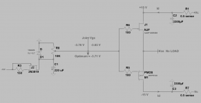
The objective of the attached schematic is to restore the design conditions which were reported earlier; shown below. It shows two 10K variable resistors to bias the FETs. Each 10K resistor gives its FET its desired Vgs. Thus, SJP120R085 got a Vgs = -3.76V, and IRFP9140 got a Vgs = -3.65V. Consequently, this modification enabled a drain current[Id] of 0.6A in each FET and a ~0 V output DC offset [+10 mV] at a constant Vds = +/-15 V.
This individualized bias approach is expected to deliver any target idle drain current in DEF at the maximum target Vds with the bonus of a Vos~0 V for direct coupling to the loudspeaker.
Attachments
One of the charms of the DEF amp is that there would not be a bias circuit,
but if you can't get an adequate match and you don't like my other trimming
technique, then this is a perfectly fine way to go.
Thank you for your valuable comments, and direction. I [mistakenly] thought a bias circuit is needed; until I read the above. My setup is still in place. I'll disable the bias circuit and report on the resultant charm of the DEF. I am glad to say that I did not ignore/or dislike your trimming techniques. I am learning DEF and clearly lag behind your knowledge of it. I hope to explore them soon.
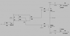
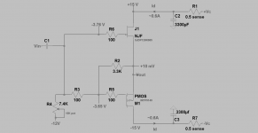
The trimming technique suggested by Mr. Pass in his BAF 2016 presentation; part 2 [towards its end] was used for the DEF under study. I adopted it as it is highly effective for its simplicity.
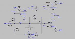
The attached schematic shows the "trimmer" to be a voltage divider. It starts at the power output node, uses the series-connected resistors 3.3K, 100 Ohm, and a 10K variable adjusted to 7.4K. It finally terminates at -12V. It works as follows:
1. The voltage at the power output node must be at 0 Vdc [+10 mV] for the direct connection to the loudspeaker. So, the current flowing through this voltage divider is 1.1 mA.
2. A 3.3K resistor is connected betwen the output and the gate of P-MOS. The resultant voltage at its gate [Vgs] is -3.65 V as determined earlier.
3. The voltage after the 100 Ohm resistor goes to the gate of R085. This Vg is -3.76 V as determined earlier.
4. The drain current [Id] flowing through both FETs was found to be the design value of 0.6 A.
5. Another interesting benefit of the trimming technique by Mr. Pass is the high impedance which is presented to the preceding preamplifier; due to bootstrapping.
I am ready to listen to this DEF at low output level.
Attachments
The trimming technique suggested by Mr. Pass in his BAF 2016 presentation; part 2 [towards its end] was used for the DEF under study. I adopted it as it is highly effective for its simplicity.
The attached schematic shows the "trimmer" to be a voltage divider. It starts at the power output node, uses the series-connected resistors 3.3K, 100 Ohm, and a 10K variable adjusted to 7.4K. It finally terminates at -12V. It works as follows:
1. The voltage at the power output node must be at 0 Vdc [+10 mV] for the direct connection to the loudspeaker. So, the current flowing through this voltage divider is 1.1 mA.
2. A 3.3K resistor is connected betwen the output and the gate of P-MOS. The resultant voltage at its gate [Vgs] is -3.65 V as determined earlier.
3. The voltage after the 100 Ohm resistor goes to the gate of R085. This Vg is -3.76 V as determined earlier.
4. The drain current [Id] flowing through both FETs was found to be the design value of 0.6 A.
5. Another interesting benefit of the trimming technique by Mr. Pass is the high impedance which is presented to the preceding preamplifier; due to bootstrapping.
I am ready to listen to this DEF at low output level.
What would be the value of C1? Keep in mind I am new to all this
What would be the value of C1? Keep in mind I am new to all this
Hello joesch1999. The value of the coupling capacitor is expected to be low; maybe 5 to 10 uF, and thus can be of high quality like a polypropylene type. I do not know the value of the bootstrapped input impedance. I'll try several caps [1 to 10 uF] and determine the optimal value by ear; with focus on the loudspeaker's bass performance.
- Home
- Amplifiers
- Pass Labs
- DEF Amp