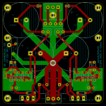
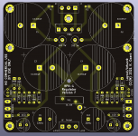
Based upon improvement suggestions I have updated version "C" (attached first) and made a new version "D" which moves the pass transistors to the left and right sides of the PCB. Unless anyone spots something I plan to order the PCB tomorrow. Today I will be further considering my chassis and deciding between "C" and "D".
Attachments
-
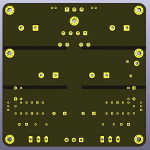
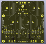 KOZARD HPA1 Regulator Version C Draft Placement Bare.png96.2 KB · Views: 235
 -
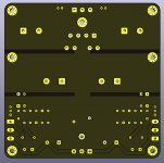
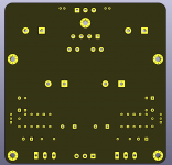 KOZARD HPA1 Regulator Version C Draft Placement Back.png35.7 KB · Views: 233
 -
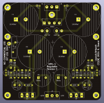
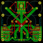
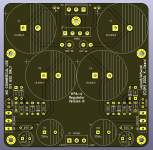 KOZARD HPA1 Regulator Version D Draft Placement Bare.png98.5 KB · Views: 242
 -
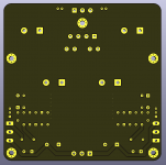 KOZARD HPA1 Regulator Version D Draft Placement Back.png41.6 KB · Views: 228

I would suggest you go back to basics here before sending the design off and start with using just 1 layer for layout and keep the 'ground plane" as free of tracks, connections etc as possible - the intial tracking should focus on avoiding any mixing of areas of high current and low current - do it in stages
ie move the first "ripple" capacitors (C1 & C2) together, as close together as you can manage (this is where the charging current pulses are at their maximum) and remove all that other 'stuff' on the outside of this - then add the next 2 capacitors (C3 & C4) to this common power ground, and not the top copper layer - this confines all the 'noisy' charging ground currents to the one area and not spreading them all over the whole board to be transferred to the regulator section and hence the unit outputs
If you must use the any of the ground plane/top layer for the zero volt connections, minimize the ground loops - this applies even with low current use.
Where is your 'power ground' point? Or 'floating ground lift' resistor/thermistor?
Is this a good location for a thermistor?
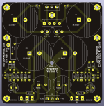
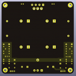
I also removed the top pour and segmented the back ground plane. Does that alleviate the charging current related noise concerns?
I also removed the top pour and segmented the back ground plane. Does that alleviate the charging current related noise concerns?
Attachments
Last edited:
The previous post was an edit on version C.
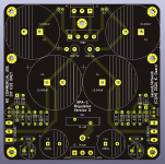
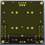
Here is version D with the back ground plane segmented. Is that enough to alleviate the charging current related noise concerns? Note that I also rotated C1 and C2 to reduce the length of the traces to C1 and C2.
This version has a different location for the thermistor. Is this a good location for a thermistor?
Attachments
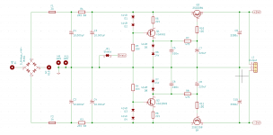
You might want to think about establishing a single point of ground. On the schematic, this would be on the wire to the right of the junction between C3 and C4. Connect the ground plane at this point and don't use it to carry any current at all. Just use it as a shield. Then, on the top side, have separate short ground buses for the positive and negative regulator sections, and connect them back to this point. And finally, a fat conductor, again to this point, going to the output connector ground. The goal is to avoid mixing positive and negative section ground currents, to keep the voltage reference grounds separate, and to also keep the output current separate with a straight path back to the filter cap common ground.
This is just an idea in my head and how I did the Super Regulator boards on my amplifier projects, posted elsewhere. Seems to work, though I haven't proven it with measurements.
FWIW and YMMV.
Edit: Though based purely on theory, I like to keep ground currents confined to well-defined paths, and to try to arrange them so that the resulting voltage drops don't affect anything. I'm not that keen on isolation slots in ground planes. They just force the currents to go through longer paths. Other people have had good success with ground plane design. I don't represent myself as an expert.
Last edited:
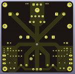
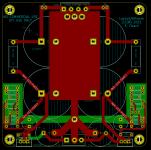
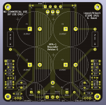
Ok. Please take a look at the attached version. Is this along the right track?
Attachments
Last edited:
Attached is the other version with the pass transistors on the left and right sides.
Hopefully all these changes are for the better. Plan is to order tomorrow.
Hopefully all these changes are for the better. Plan is to order tomorrow.
Attachments
Interesting changes. Yes, definitely more along the lines of what I was thinking, but maybe a little too busy. Let me catch up with you via PM. Hopefully someone else will weigh in; there's a lot of talented people reading this thread, I think.
One suggestion based on my own experience. Seems like you're still heavily iterating. I wouldn't be in a rush to order boards if you can afford to wait. I have a rule now which is I sit on my layout for at least a week once I'm absolutely sure it's "perfect." I look at it once a day while I'm waiting, and I always find several errors and/or things I can think of to optimize. I only order when several days have gone by and I can think of absolutely NOTHING else to change. I might find minor corrections after I commit the order, but hopefully not show-stoppers. Before I had this rule, I think it was three times I had to send boards directly to the trash when I got them because of problems I discovered while I was waiting for them to arrive.
Edit: Yes, thinking about it, you need to do a better job isolating the "dirty" charging currents in the first stage filter caps from the "clean" ground you're trying to establish for the regulators and output terminal. I'll see if I can explain in my PM, which I'm writing now.
Last edited:
Ah, that's better - I can now see what you're doing, not guessing.
I can't emphasize the significance of getting the C1 & C2 0v terminals close together with very low impedance between them and keeping this point of max charging currents away from the rest of the circuit - it's absolutely essential, especially in a preamp amp headamp.
Now I know it requires a bit of a change in the layout but I think we can still get it all onto that size limitation as there's still quite a bit of open space there - it's really good that you've numbered/lettered each version so you can easilt go back to previous versions as sometimes they are actually better - we've all been there ...
Okay, firstly, using a "star point" for the power supply ground is NOT the best way of developing power supply pcbs but it IS useful elsewhere - see the "Tentlabs Papers" about this for a reference, amonget others.
Iusually put the positive to the right side but that's not a big deal.
Okay, on you design svreen, move the ac bits off the layout for now and move the C1, C2, C3, C4 together with maybe a few mm apart if you might want to try bigger dia caps - this puts all 4 0 volt terminals close together so make this a high current closed loop with a rectangle with just one 0 volt connection to the transformer, or maybe 2 if using 2 separate secondary transformer windings - to save board space, use 1/4" spades instead of 3 pin terminal - this also allows to separate the input terminals for the other ac input ytansformer terminals that might be useful.
Now, the block bridge can go to the edge of the board and as it has 'long legs', this can actually hang over outside the pcb edge so can go between the C1 and C2 without heating the caps, or even maybe attaching a heatsink if required for some other higher current application. Now the 2 ac input 'spades' can go towards the outside perimeter of those same C1 and C2 caps so these caps can still be 'close to the top' of the board.
Now there's a lot of discussion about keeping the 0v ground together for the C3 and C4 in a C-R-C circuit but suggest keep them all 4 of them together and also keeps them all oriented the same way - reduces potential mistakes, maybe later too - I've done this simple thing myself so ...
Okay, this little high current charging network is virtually 'self contained" and each cap is getting 'punched' every 1/120th second with a short current pulse that means each of the caps gets a pulse in turn, not together, like a horizintal Porsche engine and this means there's a small potential between the caps 0 volt terminal across that copper track separating them - ir the engine crankshaft, if you're okay with the analogy.
Now, the resistors of the "R" in the C-R-C can go on the outside perimeters of the caps too - again, you have some spare space so maybe add donuts for using 2 resistors in parallel if you want to change this "R" later on. Adding options, you see, easy to dump them in not required.
Now, back to our engine analogy - connecting the crankshaft to the gearbox use and auto exchanger (fluid clutch, etc, etc) - this uses a strip of the copper to produce a small increase in resistance so you "looking to have this" about half the size of the distance between the caps 0 volt terminals, depending on the required max current draw of the supply - oin your pcb designer, there's a calculator for track resistances and inducrance, etc - the 'strip should be about twice the resistanse of a couple of milli-ohms - sound silly, but it makes all the difference.
Okay, now you have the low ripple regulator section and you're looking for it's 0 volt ground point at the output of the pcb, NOT the centre of that 'star earth" - another point of conjecture so quite a few different ideas about this too, depending a lot on the 'end use' not so much about which one is "correct" or right - this includes mine too!
The only extra I would suggest you look at is to again think about 1/4" spades for the output terminals - they require adding the terminals to the connecting (plus sleeves maybe too) but less space, more options etc at this design stage
Sorry for all the words and maybe you'll find some of the ideas useful - all the best.
Ok. Let me know what you think of this version.
I think I incorporated everything except:
I think I incorporated everything except:
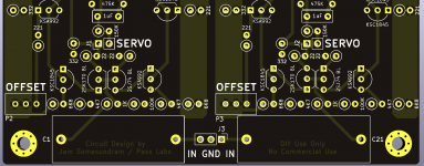
- The thermistor (or bridge/resistor) would be externally added using the via to solder an optional wire. This is to accommodate the variety of requests that I received.
- Please also explain how to pour the shield only ground plane (and maybe quickly sketch exactly where to put it). When KiCad pours the ground it connects it everywhere so I am not sure how to draw it as a shield only (without connections). I assume I should just make it another net and use a zero ohm or jumper to connect it?
Attachments
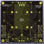
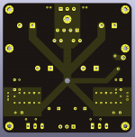
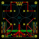
Ok. So I used a shorted two terminal solder jumper (on the back) to connect a poured shield to the central (front side) ground pour using a via.
The front did not change (from the last post). This new image shows the shield and the jumper on the back. Is this the right place for the shield and also is it the best place for the shield connection?
The front did not change (from the last post). This new image shows the shield and the jumper on the back. Is this the right place for the shield and also is it the best place for the shield connection?
Attachments
Last edited:
Nice work, kozard. This is starting to feel more "right" to me. I don't have the time to make drawings for you, unfortunately. Shields and ground planes and such aren't necessarily all that important. My advice is to keep it simple, hone your intuition, keep seeking input, and refine your design according to your instincts. This is DIY, so you gotta "do it yourself," LOL.
Edit: Looking some more, one suggestion: Don't ground the PS through the standoffs to the chassis. Leave it to float.
Edit: Looking some more, one suggestion: Don't ground the PS through the standoffs to the chassis. Leave it to float.
Last edited:
That looks to have taken care of things, nicely done.
Good point about the non-grounding' standoffs, 'Mr 'h' - far too often done!
Now, the pcb - what I do is to leave it alone for a day/week and then come back and play around with it some more just to see if any wierd ideas come to mind and/or compare this "G" version with your earlier "D" version to see if anything is missed. I often do.
For example, if your board is to have standoff supports around 10mm (1/4 - 1/2") then you could use the longer pins on the ac bridge terminals to add a 2 pin terminal connector under neath and allows a bit more crowding of the caps C1 & C2 if the bridge is pushed right to the edge, you could move the fuses towards the mounting holes or even use the basic larger fude-holders, and so on - trimming things a bit.
Mind you, you can play with these things forever and never complete the projects too - that's me!
About ground planes - I tend to avoid using any ground plane around the charging circuit 'bits' to avoid picking up any 'noise' from the diodes/bridge and tracking and keeping it from 'bleeding' into the main power supply ground - other people do just the opposite to try avoiding/reducing any of this 'noise' radiating into ither nearby circuits
Why look at these and other options? Well, firstly, if you're happy with this design, why not see what else you might use it for?
Perhaps driving a class A power amp with the big 10mF ripple/smoothing caps, for example. You might increase the width of the tracks a bit for this if you're looking to run say, 1 - 2 amps thru this supply/filter instead of the HPA-1 draw of about 100mA
If you ever get around to designing pcbs where you might mount thru hole components, yerminals, etc underneath here's something I recently did you might avoid - one of the bottom mounted resistor's ends was soldered under a capacitor as a track layer jumper (bottom layer to top to avoid relying on a 'via' under a cap - you can't check this for track continuity) and after soldering the resistor and trimming the legs, there was enough left to penetrate the insulation when I fitted the cap and caused quite a lot of 'head-scratching' - just a simple mistake when 'squashing' component density but the something we can learn to avoid in future.
Oh yes, I think your 'KiCad includes those fancy donuts that have little fingers on them to avoid the application of high heat to solder the power caps terminals - the bigger the tracks, more heat to solder and these donuts reduce the heat a lot - especially useful if you might want to change those caps for any reason.
Some people like to use the power cap's terminals as 'vias' or 'layer changers' as there's generally quite a bit of spare space around these bigger components and convenient place to do it - I try to avoid this because if you even need or want to change these caps, it very easy to pull that 'via' out with the solder/capacitor pin and becomes a real PIA to find the problem later on - another infuriating error of my ways!
Perhaps I might add that a friend of mine is far better at developing pcbs and I like to send my 'best efforts' to him for further evaluation before manufacture and even for simple circuits, there's quite a large improvement in the final product so we're all learning better methods each time we do our "pcb Sudoku"
Just a little something else to keep in mind - many of the 'Component Supply Chains' are either slowing or breaking down completely so some components are becoming harder to source, already harder out here in Aus, so availability of the components is again becoming significant in any pcb flexibility as a lot of say, capacitor replacements don't have the same pin spaces, similar transistor have different 'pinouts', etc and this situation isn't going to improve any time soon so, more lateral thinking and check component availability ...
") .
.
- Home
- Amplifiers
- Pass Labs
- Pass HPA-1, what do we know?