B1 problems
Thanx for the fast response. The PCB and matching JFET's were sourced from Pass DIY store. The sparts were sourced from, Nelson Pass B-1 preamp kit.
Thanx for the fast response. The PCB and matching JFET's were sourced from Pass DIY store. The sparts were sourced from, Nelson Pass B-1 preamp kit.
Attachments
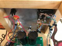
I see lots of twisted wires.
But for each the two wires are soldered onto one pad.
A twisted pair is one wire of the pair to carry the signal to the next stage and the other wire of the pair to bring the signal back to the Source. We call them Signal Hot and Signal Cold or Flow and Return.
Every circuit REQUIRES the current to RETURN to the Source. There are no exceptions to this rule.
Use your twisted pair as Flow and Return for each signal connection.
eg.
at an input RCA/Phono socket you have the Hot pin at the middle and the Cold tag at the side.
You solder one wire of the twisted pair to the Hot Pin and solder the other wire of the pair to the Cold tag.
Run this twisted pair to the next stage. The Hot wire goes to Signal Input pad and the Cold wire goes to the adjacent Signal Return pad (often mislabelled as ground, or GND). This is one signal connection using a twisted pair.
Last edited:
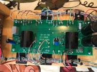
All the values were taken before the short occurred. Maybe I should explain. Built B1, B1 functioned for about 1 minute, speakers made a loud noise, like plugging in a guitar to a live amp, shut off amp, turned on amp, same noise, replaced 24vdc wall wart with 19vdc wall wart from amp camp amp, made music again, but with the speaker problem, did component check, finished, but puff of smoke rechecking q200 value.
I'm pretty visual kind of guy , so schematic with voltage values (as many you can) , all ref. to gnd - will help much more than sheet you posted
however - drill is simple :
triple check all wiring , especially polarities ;
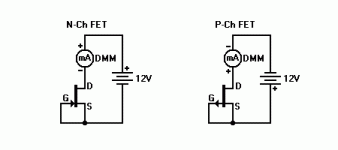
pull out all semiconductors ( yeah , plenty ..... ) and test them with simple matching jig
however - drill is simple :
triple check all wiring , especially polarities ;
pull out all semiconductors ( yeah , plenty ..... ) and test them with simple matching jig
Attachments
- Status
- This old topic is closed. If you want to reopen this topic, contact a moderator using the "Report Post" button.
- Home
- Amplifiers
- Pass Labs
- Pass B1 problems