
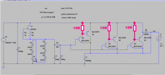
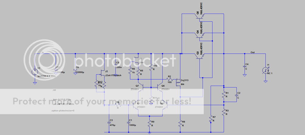
I suggest you install speed-up resistors in the collector circuits of your Sziklai input transistors. These help suck out the base charge of the PNPs when you're trying to drive the output voltage lower. A value of 15 ohms would bias the NPNs at (VBE/15) = 47 milliamps each, which seems like a reasonable starting point. I might also replace the 1 amp rated, output protection diode 1N4004, with a 15 amp MUR1520. Just to be careful.

_
_
Attachments
I suggest you install speed-up resistors in the collector circuits of your Sziklai input transistors. These help suck out the base charge of the PNPs when you're trying to drive the output voltage lower. A value of 15 ohms would bias the NPNs at (VBE/15) = 47 milliamps each, which seems like a reasonable starting point. I might also replace the 1 amp rated, output protection diode 1N4004, with a 15 amp MUR1520. Just to be careful.
_
Thanks for the tips. I will try that out.
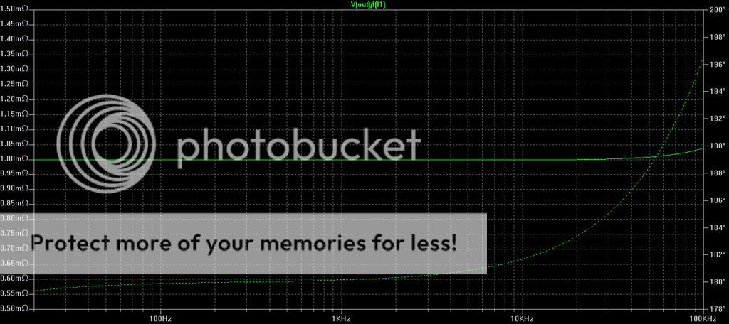
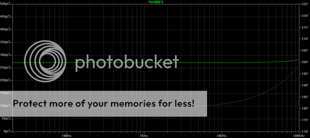
Just to avoid confusion, the impedance curves in the previous posts are for a completely different circuit. I haven't posted the circuit as yet. I will build it first.
You may find it interesting to study Nelson Pass's "STASIS" power amplifier schematic. Why? Because he, like you, chose a Sziklai topology with NPN input transistor and PNP output transistor. The full schematic is shown on this web page but it's a bit difficult to understand at first glance.
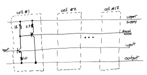
The output stage is twelve Sziklai pairs pulling the output terminal up, and twelve more Sziklai pairs pulling the output terminal down. There are also twelve positive supply rail drivers (the A8s at the top) and twelve negative supply rail drivers (the A6s at the bottom). The rail drivers reduce the VCE voltage across each output transistor.
The basic Sziklai pair for output pullup, is drawn in the figure below. Notice that Nelson Pass has decided to install local emitter degeneration resistors in both the NPN and the PNP (1.0 ohms and 3.3 ohms respectively). Is this an idea worth copying? Is this a stupid idea? Is this only relevant when you're building repeating cells of parallel Sziklais? (like the schematic in post #42 above)?
You're the circuit designer, you make the decision.
_
Attachments

I never bothered with LM399s because it seemed to me that they were a very expensive solution to a problem that I don't care about: ultra low temperature coefficient. When considering a (shunt) voltage reference IC, I am much more concerned about supply (in)sensitivity and output impedance. Both of which I can get far more cheaply with a shunt preregulator and a bog standard LM285 or LM329. Noise can be attenuated by arbitrarily huge amounts through filtering -- God did give us both capacitors and inductors to make 40dB/decade slopes -- and I'd rather do that than count on the semiconductor manufacturer + distributor to send me a unit whose noise matches the "typical" number in the datasheet.
I suggest you decide what two performance criteria are most important to you, then build up two or three test boards with different circuit designs of voltage references. Test them and measure your top two performance criteria. Whichever circuit measures best, according to the criteria that really matter to you, is the one to pick.
I suggest you decide what two performance criteria are most important to you, then build up two or three test boards with different circuit designs of voltage references. Test them and measure your top two performance criteria. Whichever circuit measures best, according to the criteria that really matter to you, is the one to pick.
It's probably not going to matter, I'm just trying to learn what might be considered the top 3 options.
I've simulated TL431, LED stack, and Zener.
My greatest concern is the observation that has been made that regulators often lack dynamics compared with a straight capacitor powersupply.
Is this because:
1) Not low enough output impedance on the regulator?
2) Not paralleling enough devices on the output of the regulator to deal with the current demands of the amp?
I can always throw 33,000uF to 100,000uF at the output of the series regulator if it is required (assuming that does not create issues for the regulator)
If this is done right it should kick **** on any CRC supply.
What software are you using?
Martin
LTspice
My greatest concern is the observation that has been made that regulators often lack dynamics
compared with a straight capacitor power supply. Is this because:
1) Not low enough output impedance on the regulator?
2) Not paralleling enough devices on the output of the regulator to deal with the current demands of the amp?
The regulator is a feedback amplifier, with all that implies. A large amount of capacitance on the output
markedly slows its response, due to creating a low frequency dominant pole with the output resistance.
The regulator is a feedback amplifier, with all that implies. A large amount of capacitance on the output
markedly slows its response, due to creating a low frequency dominant pole with the output resistance.
Yeah, I thought that could be the case.
It sounds like you need to build your power supply twice, once with "CRC" nonregulated topology, and again with active voltage regulation. Then listen to the amplifier with both options and choose the one that kicks the most *** . You're the judge and jury, nobody else's opinion matters.
I think your LTSPICE simulations might give you a pleasant surprise when you start to connect electrolytic capacitors (including their ESR and ESL!) to the output of your 3-parallel-Sziklai-pairs voltage regulator. I think you might well find that your open loop output impedance is ~ 7 milliohms, and your capacitors' ESR is ~ 10 milliohms, meaning that the output pole and the capacitor ESR induced zero are very close together, so the region of -40dB/decade slope (where instability occurs) is small to nonexistent. Thus the stability concerns raised by member rayma -- ooga boogah, negative feedback! -- might prove to be negligible in simulation. Fire up LTSPICE and see.
I hope you do intend to include ballasting resistors if you build multiple parallel output drivers; one BJT will certainly have a lower VBE than all the others and you don't want this to trigger thermal runaway. Nelson Pass's STASIS amplifier with >>twelve<< parallel output drivers, shows deep concern about transistor mismatch. Maybe it's more wisdom than paranoia (?). You be the judge.
I'm more fearlees than NelsonI hope you do intend to include ballasting resistors if you build multiple parallel output drivers; one BJT will certainly have a lower VBE than all the others and you don't want this to trigger thermal runaway. Nelson Pass's STASIS amplifier with >>twelve<< parallel output drivers, shows deep concern about transistor mismatch. Maybe it's more wisdom than paranoia (?). You be the judge.
 (He is working hard blowing up SITs trying to get into the ABFAB club hahaha).
The devices can only hog as much current as the amp draws. So they can't run away.
If the amp draws 5A then assuming 1 device hogs all current (worst case scenario) then 5A x 5V = 25W.
It is highly unlikely one device will hog all current a realistic worst case scenario might be 2/3 as a guess.
At least that's what I think. I am known for brain farts though.
Last edited:
- Home
- Amplifiers
- Pass Labs
- Developing a Regulated Dual Rail Power Supply For FirstWatt Amps