Firstly, I will like to thank Patrick for trusting me with the Beta Build and his XEN team for help in logistics and many other matters.
Some considerations before you embark on building this amp which I think will be useful to sort out first.
1)Resistive pot or LDR. This amplifier has LDR volume control provisioned on to the PCB. You will have to build the a CCS source on perf board though. This is my first experience with LDR and I do like what I am hearing, although I did not compare with a resistive pot.
2) Crossfeed module. The PCB has mounting holes for crossfeed module daughter boards. I will suggest to use pins for the associated jumpers holes such that you will be able to try out for yourself whether you like crossfeed. I tried and I love what I am hearing so crossfeed stays and will be part of all my future builds in headamps")
3) Power supply options. The board provides for 2 Talema 25VA PCB transformers and 4 3-pin IC based regulators. I am using the pin compatible 317/337 based power supply boards provided by Patrick. I will be covering the build for those as well.
The PCB also have mounting holes for batteries powered supply if you so wish
Some considerations before you embark on building this amp which I think will be useful to sort out first.
1)Resistive pot or LDR. This amplifier has LDR volume control provisioned on to the PCB. You will have to build the a CCS source on perf board though. This is my first experience with LDR and I do like what I am hearing, although I did not compare with a resistive pot.
2) Crossfeed module. The PCB has mounting holes for crossfeed module daughter boards. I will suggest to use pins for the associated jumpers holes such that you will be able to try out for yourself whether you like crossfeed. I tried and I love what I am hearing so crossfeed stays and will be part of all my future builds in headamps
3) Power supply options. The board provides for 2 Talema 25VA PCB transformers and 4 3-pin IC based regulators. I am using the pin compatible 317/337 based power supply boards provided by Patrick. I will be covering the build for those as well.
The PCB also have mounting holes for batteries powered supply if you so wish
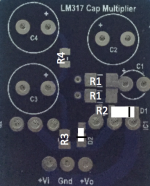
Stuffing of F5-HA mainboard
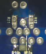
Stuff the 6 SMD resistors first (3 each channel) before proceeding with through hole components.They are found at the back of the PCB. There is actually very little components for the mainboard. Just follow the BoM and schematic and you should be fine.
One tip on soldering the 100R SMD resistors. Solder only on one side of the resistor for the first time, as shown in picture. The other side is too close to the padding for the JFET. You will likely to bridge the JFET mounting hole. You can come back to solder this side when the JEFT is soldered.
Do not solder the Jumper wire yet. It will come later.
The SOT23 padding and the resistor padding at the back of the PCB is meant for the current limiting circuit. I didn't use those so it is left blank.
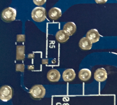
Note: R5 is not part of the current limiting circuit. R5 SHOULD be populated.
Series Resistor for LDR control goes to J21. Jumper this if you are not using LDR.
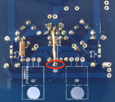
JFET should be mounted to the heatsink with thermal epoxy. I use those from Arctic Silver.
TIP: Place the JFET in place and then solder the Trimmers. Remove the JFET after which. This is to make space to adjust for the R_drain for the initial biasing, which requires you to measure the resistance between R3/R4. If you solder in the JFET, it will be very tight for the probes.
Use this equation : R_drain = (MOSFET Vgs at Bias + Bias Current x 3.3)/ JFET Idss
Eg: I am using K170/J74GR, my Idss is 5mA. I am biasing to 150mA in which the MOSFET will have a Vgs close to 5V. Hence i should measure for 1.1K ohm for the start.
Do take note to leave some breathing space for the 3.3R resistors.
Stuff the 6 SMD resistors first (3 each channel) before proceeding with through hole components.They are found at the back of the PCB. There is actually very little components for the mainboard. Just follow the BoM and schematic and you should be fine.
One tip on soldering the 100R SMD resistors. Solder only on one side of the resistor for the first time, as shown in picture. The other side is too close to the padding for the JFET. You will likely to bridge the JFET mounting hole. You can come back to solder this side when the JEFT is soldered.
Do not solder the Jumper wire yet. It will come later.
The SOT23 padding and the resistor padding at the back of the PCB is meant for the current limiting circuit. I didn't use those so it is left blank.
Note: R5 is not part of the current limiting circuit. R5 SHOULD be populated.
Series Resistor for LDR control goes to J21. Jumper this if you are not using LDR.
JFET should be mounted to the heatsink with thermal epoxy. I use those from Arctic Silver.
TIP: Place the JFET in place and then solder the Trimmers. Remove the JFET after which. This is to make space to adjust for the R_drain for the initial biasing, which requires you to measure the resistance between R3/R4. If you solder in the JFET, it will be very tight for the probes.
Use this equation : R_drain = (MOSFET Vgs at Bias + Bias Current x 3.3)/ JFET Idss
Eg: I am using K170/J74GR, my Idss is 5mA. I am biasing to 150mA in which the MOSFET will have a Vgs close to 5V. Hence i should measure for 1.1K ohm for the start.
Do take note to leave some breathing space for the 3.3R resistors.
Attachments
Last edited:
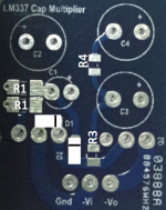
Stuffing of F5-HA power regulator modules
The PCB Patrick designed is very compact, uses SMD components extensively. You should be comfortable with SMD soldering before proceeding. Try out on some old boards if required.
You will need some sharp tipped soldering iron, lots of flux and sharp tweezers.
The following build order is highly recommended as the board is tiny. Especially the MSE1PJ diodes. The spacing between the anode and the cathode is 0.5mm. Hence it is crucial you check your work with a diode tester before proceeding.
1. MSE1PJ diodes
2. 240R resistors
3. All other resistors.
4. SMD BC817/BC807
5. Electrolytic Caps
6. TO-220 devices.
TO-220 devices should be aligned properly with the mechanical parts of the chassis before soldering. Measure twice, solder once. You will very likely damage the boards/components if you have to desolder.
Use the following silkscreen to assist you. The diode has a cathode marking. Follow as per diagram.
This is Patrick's advice on soldering of the MSE1PJ diodes which I have used myself.
"When I did my soldering, I use a pair of sharp tweezers to grip the diode exactly at the gap.
Then place the diode on the PCB, using the tweezers as alignment indicator.
A bit fiddly, but 100% success."
Use flux to help hold the device in place and to allow solder to flow. Look up on videos for SMD soldering and practise on old boards if you need to.
After soldering the diodes, make use of the LM317/LM337(Labelled IC1) mount points to test the connection. You should get approximate 0.53V forward bias with the diode test function. When satisfactory, you should solder R2, 240R resistor next, as it is positioned beside the diodes.
After assembly, mount the modules on a heatsink and test it with a bench power supply to ensure the board output the required +- 15V
Attachments
Last edited:
There is a quite a number of jumpers on the board. 2 are absolute necessary and it is required to be soldered on before we can test the mainboard. Once the mainboard is tested ok, we can proceed for the rest of jumpers.
The two crucial jumpers connects the output ground to circuit ground and can be found at the back of the board. I made use of enamel coated copper wire to prevent possible shorts. One note on the jumper, the wire should protrude out at least 5mm in the place where I circled. This is the Out ground and it goes to your headphone jake. Pls be mindful of this. If not you will not be happy. You have been warned
Once you have mounted the 2 crucial jumpers, checked all soldering joints are free of shorts and the MOSFET soldered and mounted on heatsinks, you can do the initial test and biasing.
It is advisable to use a dual rail lab power supply for this. You can limit the current to prevent any potential damage if the board is oscillating. Set the limit to 200mA, +-15V.
If you are not using batteries, use the batteries mounting holes to power the board(V+ , Gnd, V-) . This saves you the trouble of desoldering later.
Biasing procedure
Short the input to ground. Your task will be a lot easier if you have 2 DMMs. Strap 1 DMM across one of the 3.3R resistor of the side you are biasing (This DMM measures voltage across 3.3R which is used to determine bias current) and 1 DMM across the Vout and Gnd(This DMM measures DC offset)
Turn one trimmer(annotated as T1 from this point) to your desired bias. You will notice that the output offset is likely to increase. Adjust the other trimmer(T2 from now on) to halve the offset. After which, go back and adjust T1 to 0V offset. Re-adjust the bias if needed. Let it warm up for another 30 minutes, you will notice the bias should have drifted. Readjust if needed so that the bias is the same for both side. DMM should read 0.5V for 150mA bias. Use this calculation for your desired bias.
Bias Current * 3.3 = Reading on DMM
Repeat the same steps for the next side.
Testing of boards
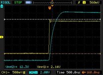
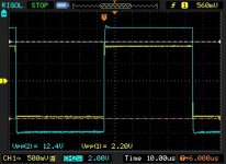
Once you are happy with the offset, you may proceed to test the board with a oscilloscope. Start off 2V pk to pk 1kHz square wave at input. Output without load will be 12V pk-pk with no ringing/over shoot. Increase MOSFET gate stoppers R5/R6 should cure the ringing. Once the waveform is clean, you may wish to check again with a dummy load.
Note the attached waveforms on my build. Yellow is input, cyan output. The slight ringing is due to my cheap DDS signal generator.
The two crucial jumpers connects the output ground to circuit ground and can be found at the back of the board. I made use of enamel coated copper wire to prevent possible shorts. One note on the jumper, the wire should protrude out at least 5mm in the place where I circled. This is the Out ground and it goes to your headphone jake. Pls be mindful of this. If not you will not be happy. You have been warned
Once you have mounted the 2 crucial jumpers, checked all soldering joints are free of shorts and the MOSFET soldered and mounted on heatsinks, you can do the initial test and biasing.
It is advisable to use a dual rail lab power supply for this. You can limit the current to prevent any potential damage if the board is oscillating. Set the limit to 200mA, +-15V.
If you are not using batteries, use the batteries mounting holes to power the board(V+ , Gnd, V-) . This saves you the trouble of desoldering later.
Biasing procedure
Short the input to ground. Your task will be a lot easier if you have 2 DMMs. Strap 1 DMM across one of the 3.3R resistor of the side you are biasing (This DMM measures voltage across 3.3R which is used to determine bias current) and 1 DMM across the Vout and Gnd(This DMM measures DC offset)
Turn one trimmer(annotated as T1 from this point) to your desired bias. You will notice that the output offset is likely to increase. Adjust the other trimmer(T2 from now on) to halve the offset. After which, go back and adjust T1 to 0V offset. Re-adjust the bias if needed. Let it warm up for another 30 minutes, you will notice the bias should have drifted. Readjust if needed so that the bias is the same for both side. DMM should read 0.5V for 150mA bias. Use this calculation for your desired bias.
Bias Current * 3.3 = Reading on DMM
Repeat the same steps for the next side.
Testing of boards
Once you are happy with the offset, you may proceed to test the board with a oscilloscope. Start off 2V pk to pk 1kHz square wave at input. Output without load will be 12V pk-pk with no ringing/over shoot. Increase MOSFET gate stoppers R5/R6 should cure the ringing. Once the waveform is clean, you may wish to check again with a dummy load.
Note the attached waveforms on my build. Yellow is input, cyan output. The slight ringing is due to my cheap DDS signal generator.
Attachments
Last edited:
Jumpers
The last few steps you need to do is installation of jumpers.
If you are making use of the regulator mounting holes, you will need to install 1210 0R jumpers at the designated padding. Or you can use copper strips. Your choice.
For the various jumpers on the top side of the board, it will be determined by whether you are using crossfeed or whether you are using LDR volume control.
Follow the attached diagrams based on your configuration.
If you are using LDR volume control, the series resistor should be soldered in J21. If not using LDR volume control, jumper J21.
Note: If you are using LDR volume control, but not the crossfeed, you should increase the serial resistor to 10K to compensate for the gain. Crossfeed will reduce the input signal by a factor of 3 and hence if you did not use crossfeed, the proposed 5k series resistor will be too low.
The last 2 jumpers are found on the padding beside J1 and J4. These are the additional signal shielding and should be connected based on the following configurations. The padding is for 1206 resistors.
When using crossfeed, use a 0R resistor for right channel Gnd Plane bridging resistors, left channel open.
When not using crossfeed,
3-wire output, use 0R resistor for right channel Gnd Plane bridging resistors, left channel open
4-wire output, use 0R resistor for right channel Gnd Plane bridging resistors, left channel use a 10R resistor
Attachments
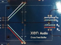
Crossfeed
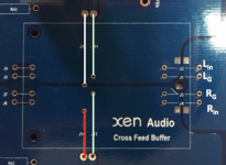
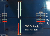
The crossfeed module I am using is the modified Danyuk board.
In addition to the crossfeed module, you will need a +-8 V power supply built on perf board. I use a simple 78L08/79L08 power supply.
Stuff the PCB with components of your choice according to the BoM.
For crossfeed to work, they will need a common input ground. Thus both input ground goes to Gnd, L+ goes to Lin and R+ goes to Rin.
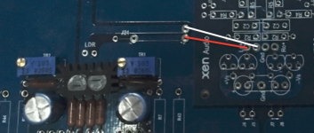
For output to mainboard, use the following picture. The picture shows wiring for the left side. Repeat for the right.
The crossfeed module I am using is the modified Danyuk board.
In addition to the crossfeed module, you will need a +-8 V power supply built on perf board. I use a simple 78L08/79L08 power supply.
Stuff the PCB with components of your choice according to the BoM.
For crossfeed to work, they will need a common input ground. Thus both input ground goes to Gnd, L+ goes to Lin and R+ goes to Rin.
For output to mainboard, use the following picture. The picture shows wiring for the left side. Repeat for the right.
Attachments
Last edited:
Finale : Music
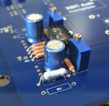
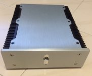
Once everything tests proper, its time to mount the transformers on PCB, power supply modules onto the chassis heatsink and then it is time for music
My humble impression of the amp:
This is my first time writing my impression so do forgive me if its not up to par. I am using a pair of HD650 and my previous amps was a Cavalli Audio EHHA Rev A hybrid. Comparisons are between these two amps.
Bass deeper with more impact. Vocals are sweeter. Soundstage is much wider, pinpoint precision in an orchestra. I can tell exactly where individual instruments are situated. Very very engaging music especially with plucking of strings in cello, drawing of strings in violin. I can hear and feel clearly as each string is being plucked or drawn.
A darker background which allows much more details to be heard.
Impression of crossfeed:
Concert pieces sound as I am in the concert hall. Music sounds more natural, less of the "in your ear" feeling.
No more "headphone" fatigue
Reminds me of the speaker set up. Definitely a keeper.
Phenomenal headamp! I have never heard my HD650 sound so good. I will recommend this to anyone without hesitation.
I'm totally mind blown! I never thought much about solid state, often refer them as lifeless amps. This amp is so so full of life.
I'm now a convert
Looking forward to the next project : The DAO head-amp
Attachments
Matching of devices
To lower the offset as much as possible, the 3.3R should be matched and ideally 4 point probe matched. I do not own a 4 point probe tester so this is what I did.
Current is provided by a 1.5V battery. Use a resistor in series to lower the supply current if you wish. It is good to purchase more of 3.3R resistor for matching. With some luck, 10 pcs will yield you 2 matched sets.
Matching of output MOSFET
I used FQP3N30/ FQP3P20 complementary Fairchild MOSFETs as recommended by Patrick
F5 Headamp?.
The devices are Vgs matched at 3 different Id (100, 150,200). This will give a better match then single point Vgs match.
The yield is low. Out of 30 pair of devices, I managed to get 3 sets of NNPP Quad match at +-0.10 Vgs
Pictures of the build process
This is the partially populated LM337 power supply. Notice how small the components are. The resistors are 0805 susumu. Be extra careful not to make a mistake here. I, for one, won't want to be desoldering these boards
This is the partially populated main board taken with the crossfeed board placed onto it. There is more stuff at the back
An externally hosted image should be here but it was not working when we last tested it.
An externally hosted image should be here but it was not working when we last tested it.
This is the partially populated LM337 power supply. Notice how small the components are. The resistors are 0805 susumu. Be extra careful not to make a mistake here. I, for one, won't want to be desoldering these boards
An externally hosted image should be here but it was not working when we last tested it.
This is the partially populated main board taken with the crossfeed board placed onto it. There is more stuff at the back
Last edited:
An externally hosted image should be here but it was not working when we last tested it.
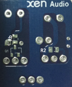
Front of side of the left channel. The 3 components in the foreground is for the providing a 9V CCS for the LDR. Notice the pot mount holes for the LDR CCS? This is for mounting a potentiometer pointing "downwards". The shaft is then connected to a thumb dial outside the chassis. This results in the clean symmetrical "No Potentiometer" look of the chassis. Very cool feature I loved it.
An externally hosted image should be here but it was not working when we last tested it.
Front Side of the right channel. Provisions had been provided for crossfeed power supply. As mentioned, you will need to build a +- 8V power supply. Source power should be tapped from these ports.
The GND beside the Vo+ is where the jumper wire should extend at least 5mm as mentioned earlier. Same for the left channel.
An externally hosted image should be here but it was not working when we last tested it.
Back of the boards, identical for both channels. Compact and tight spacing, be extra careful
An externally hosted image should be here but it was not working when we last tested it.
This is how you can make use of the battery holes to test your setup. I listened to music for a couple of days in this manner while waiting for chassis to arrive.
An externally hosted image should be here but it was not working when we last tested it.
The completed Amp. Those black boxes in the middle are Vishay Metal Foil resistors for the crossfeed.
Last edited:
The idea of not providing PCBs for the LDR CCS and the Cross Feed regulators are two folds :
a) there are numerous different circuits or regulators for the cross feed, and CCS for driving the LDRs;
b) I do want to retain a touch of true DIY in this.
You can also see that heat from the rectifiers and the regulators are conducted to the heat sinks by aluminium angles.
That from the MOSFETs goes through the bottom plate.
Patrick
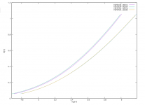
We curve traced a set of MOSFETs measured by Cloud85 with his very simplified method.
Our standard method traces all the way to 1A, which is of course far beyond the operating region of the F5-HA.
You can see that :
1) the method is still very effective in finding matched devices;
2) the difficulty in getting perfectly complementary devices.
The only solution to perfect even-harmonics cancellation is a F5X-HA.P
And even then, it is only meaningful if your source is balanced, and your headphone has 4 separate wires.
Patrick
.
Attachments
I'll use 2SK2013/2SJ313 for my build, and selected these 2 pairs (the curves were just taken at room temperature, but hopefully the MOSFETs won't get too hot with 150mA bias).
And some forum members are still offering NNPP matched set of these Toshibas.
(the curves were just taken at room temperature, but hopefully the MOSFETs won't get too hot with 150mA bias).And some forum members are still offering NNPP matched set of these Toshibas
.Attachments
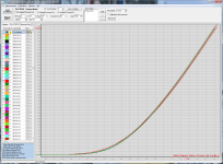
Very well matched MOSFETs.
You MIGHT need to adjust your gate stopper values for perfect square wave.
And you also need to match the JFETs for both Id & Yfs for perfect cancellation.
That means if you are using 2SK170/2SJ74, you need to use the 5.1R degen as described in the F5X Power Amp.
Or use a true complementary JFET pair (also published there before).
Patrick
For the BJTs (2SC4739/2SA1837) in the capacitance multiplier, can I use other substitutions?
I have some spare 2SC4883A/2SA1859A, pretty similar spec as the 2SC4739/2SA1837 but hfe somewhat lower (mine measures around 145 for both N and P parts). I also have some MJE15034/MJE15035, hfe is probably closer to the Toshibas (measures around 245 and 175), but Cob is higher and Ft is rather slower at 30MHz.
Thanks and regards.
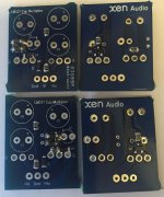
Work in progress
To continue the SMD topic from the main thread, with the aid of a magnifying glass, it's do-able even for a SMD novice. It took me 2 hours to solder only 36 components, and the soldering look pretty ugly, but I measured each component (except the BC807/817) after they're soldered and they seem OK. Hopefully they're going to work.
Maybe we should move all these building discussions to the build thread next time.
To continue the SMD topic from the main thread, with the aid of a magnifying glass, it's do-able even for a SMD novice. It took me 2 hours to solder only 36 components, and the soldering look pretty ugly, but I measured each component (except the BC807/817) after they're soldered and they seem OK. Hopefully they're going to work.
Attachments
- Status
- This old topic is closed. If you want to reopen this topic, contact a moderator using the "Report Post" button.
- Home
- Amplifiers
- Pass Labs
- F5-HA Build Thread