1) Is the amp cap-coupled at the inputs?
2)
The resistors from the outputs to ground should be about 300 times less than that. I'm not sure where the idea for 10k at the outputs came from, but in the original schematic I think you'll find something closer to 33 Ohms, plus or minus a bit. (I don't have a copy of the schematic with me--I'm quoting from memory.)
You might want to take a look at the original thread.
Grey
2)
JBL4435 said:
They are only 10k.
What about the absolute DC offset?
I think it is far too high in my case
The resistors from the outputs to ground should be about 300 times less than that. I'm not sure where the idea for 10k at the outputs came from, but in the original schematic I think you'll find something closer to 33 Ohms, plus or minus a bit. (I don't have a copy of the schematic with me--I'm quoting from memory.)
You might want to take a look at the original thread.
Grey
GRollins said:1) Is the amp cap-coupled at the inputs?
Grey
No
GRollins said:The resistors from the outputs to ground should be about 300 times less than that. I'm not sure where the idea for 10k at the outputs came from, but in the original schematic I think you'll find something closer to 33 Ohms, plus or minus a bit. (I don't have a copy of the schematic with me--I'm quoting from memory.)
You might want to take a look at the original thread.
Grey
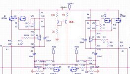
R1/4 44/45 are 47 ohm. R19/R29 are 10k
Input coupling caps aren't necessary. Their absence won't cause your problem by itself.
The input protection diodes aren't necessary either and their absence won't cause your problem directly either. However, it's easy to to destroy one or both of your input MOSFET's by static if the diodes aren't installed. The Vgs for the IRF9610 is about 4V. Hmmmm. Maybe you've got one blown input transistor.
Again let me ask the question: Do both of your channels exhibit the same 4V relative offset.
Graeme
Hello Graeme,
I have only 1 block finished.
The input Fets seem to be ok. I measure 4.9V across R23 and R25.
Now the most weird thing:
I measure around 0,56V across all source resistors (Q1, 2, 10 and 11). Slightly more than 7 Amps bias.
BUT!! Q2 and Q11 get hot after a while as they should be (app 50°C). Q1 and Q10 remain 38°C.
I know this is weird as the current is the same. But that's what is happening here
OK, no progress from your side but some from mine.
I added 2.2uF caps to the inputs. This solved the problem with the 2.2V DC offset in RCA mode.
Balanced or unbalanced I measure now 50mV DC offset. I think this is fine. Is it?
I also changed R12/R34 from 1.3 to 1kohm. Didn't measure the current gain yet but think I need to go even lower.
But I still measure 3.4 V absolute DC offset. No chance for drop. Not in the last 3 hours
Does anyone else also have this problem?
The amp sounds fine though but I think absolute DC offset shouldn't be so high.
50mv relative offset at speaker terminals is fine.You should be able to adjust the absolute offset within a few hundred mv although it will drift.If you cannot then you have something wrong.Absolute dc offset should not really affect the sound much apart from the amp clipping slightly earlier at high levels.

Hello altogether…
Since half a year I wanne built an AX.5 design but had absolutely no time to work on it.
Last week I have finished the output board and UGS layouts and the matching of the output mosfets.
Now my main problem is the bias voltage circuit:
The amplifier should have a stand by circuit (because of the monster inrush current and the electricity bill) which leave the output stage in a small conducting state while the front end is shut down.
I have done a long catalog of questions. Hope that Mr. Pass or one of the experts out there would answer to it.
1) What is the power consumption of one mono block of a commercial AX100.5 in stand by mode?
2) Are there bootstrapping capacitors implemented to get more voltage swing out of the front end? Is that generally possible?
3) Does it make sense to modulate the front end cascode devices?
(I am searching an application for the two elcaps in the original bias circuit)
4) Mr. Pass / You told me for half a year that the output of the front end is loaded by 10k resistors to each rail. Are these 3W power resistors?
5) Is the thermistor in the voltage bias circuit for faster warm up / less bias drift or current limiting for the output stage?
6) How can I drop down the dissipation of a TL431 voltage reference? My calculations show a dissipation of about 200mW when it is driven by the UGS module. Isn`t this a bit to much for a TO-92?
7) For what is the third cable (blue) in the screw clamp beside the two extern turn on cables on the mainboard?
8) Are there any plans on Passlabs for an INT-30A? (Same topology / circuit and case like an INT-150 but only 30W@8Ohm class A)
Best regards
Dirk
Forgot: There is a pass consulting internet side. They use exactly the same PASS logo as you on your new equipment - just google pass!!!???
Forgot: There is a pass consulting internet side. They use exactly the same PASS logo as you on your new equipment - just google pass!!!???
Dirk its first hit on google.de not co.nz or probably other sites.
they are travel management consultants, but
i think closet pass labs freaks like many of us
http://www.pass-consulting.com/internet/index.html
noisefree said:Now my main problem is the bias voltage circuit:
The amplifier should have a stand by circuit (because of the monster inrush current and the electricity bill) which leave the output stage in a small conducting state while the front end is shut down.
1) What is the power consumption of one mono block of a commercial AX100.5 in stand by mode?
2) Are there bootstrapping capacitors implemented to get more voltage swing out of the front end? Is that generally possible?
3) Does it make sense to modulate the front end cascode devices?
(I am searching an application for the two elcaps in the original bias circuit)
4) Mr. Pass / You told me for half a year that the output of the front end is loaded by 10k resistors to each rail. Are these 3W power resistors?
5) Is the thermistor in the voltage bias circuit for faster warm up / less bias drift or current limiting for the output stage?
6) How can I drop down the dissipation of a TL431 voltage reference? My calculations show a dissipation of about 200mW when it is driven by the UGS module. Isn`t this a bit to much for a TO-92?
7) For what is the third cable (blue) in the screw clamp beside the two extern turn on cables on the mainboard?
8) Are there any plans on Passlabs for an INT-30A? (Same topology / circuit and case like an INT-150 but only 30W@8Ohm class A)
Dirk,
Do you really expect NP to help you in what amounts to a micro reverse engineering of his shipping product? I think not and it is not really in the spirit of DIY experimentation, i.e. learning for one’s self.
That said, you raise some interesting points which I will try and answer although I should say that I do not have access to an AX100.5 and these are just my opinions.
You say that you think the standby circuit exists mainly to limit the large inrush on switch on. Are you sure? This is something that has to be handled anyway as switching on from cold will cause a large inrush due to the charging of the PS capacitors. I suspect that it might be more to do with getting the amp to warm up more quickly and reach optimal performance.
1) I’m afraid I have no idea but I would hazard a guess of something around 5-10mA per output device, i.e. a total of 5-10W.
2) I doubt it. More likely the front end (UGS) is using a higher voltage PS to fully drive the output stage.
3) Unlikely in this application and with the typical FETs used.
4) Why does it matter if the 10k resistors are 3W or not? They will typically see about 20v across them (assuming you connect to the output PS), i.e. about 40mW so I don’t see why they would need to be 3W.
5) I didn’t know there was a thermistor in the bias circuit but perhaps it has something to do with the standby arrangement. Have you considered how this might work?
6) I too have wondered about this, always assuming it is a TL431 that is used. The only way to reduce the dissipation of which I am aware, would be to use a resistor in parallel to take some of the current.
I’m in no position to answer the last two questions.
I’m also in the process of (slowly) building my interpretation of this amplifier but I haven’t given any thought to a standby option so far. Even so, it would be interesting to speculate on how this might be achieved and what benefit it might provide.
Ian.
Dirk,
Just noticed this in the XA.5 information on the Passlabs web site:
"New bias circuit – A newly developed bias generator has eliminated three sources of variation in bias current in the output stage. It also allows approximately 20% greater power output for a given supply voltage"
so perhaps you are on to something with your thermistor idea. Certainlly worth thinking about.
Ian.
- Home
- Amplifiers
- Pass Labs
- Aleph-X builder's thread.