AudGuy,
If you received LSK170's and installed them on Q3, Q4, therein lies your first problem. They need to be replaced with the appropriate JFETS in the designated spots as detailed in the BOM. I would reorder from the diyaudio store.
Next, to clarify what 'measure across' means. It means you put one of your DMM leads (i.e. red) on one end of the resistor and put the other DMM lead (i.e. black) on the other end of said resistor.
When measuring across R2 for setting bias, don't worry about the polarity that the DMM reads, just the absolute value. In other words, 0.5V is the same as (-) 0.5V in this instance.
When you are measuring for offset, use another DMM and put the red lead attached to the red binding post (+) and black lead attached to the black binding post (-).
I am assuming that your DMM leads are appropriately attached to the DMM. In other words, the red lead is attached to the "V" terminal and the black lead to the "COM" terminal. Make sure you also set the DMM to read DC volts. Frequently that is designated by a straight line with 3 dashes underneath. AC volts setting looks like a squiggle or mini sinewave.
What value (in ohms) are R7 and R8 in your build? I have a feeling that from your description of 1002F, that they are 10K ohms. Using 3K to 5K ohms may make the bias procedure easier.
One other point. Make it a habit to try to measure each of the passive components so that you do not accidently install the wrong resistor/capacitor on the pcb. Whether it is from Mouser, Digikey or even as a full kit from a known source (i.e. the diyaudio store) I always measure on my own as mistakes do happen (and quite often actually). For example, a 10K resistor and a 1K resistor look exactly the same to the untrained eye. It is important to measure each of these resistors to distinguish them. I do the same for capacitors (up to a certain value like 1000 uf) as well as semiconductors if possible.
Please post pics at your earliest convenience.
Best,
Anand.
Last edited:
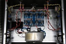
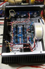
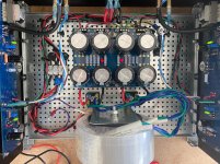
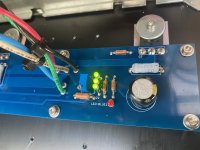
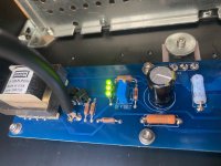
Here is a shot looking straight down at the F6 and another that is 90 degrees around.
I will post some better shots after supper, or tomorrow.
Re the JFET's . . . I though that I was ordering the correct items, but live and learn. I will see about obtaining the correct items.
Thx for answering the measuring across question, terminology can sometimes get in the way.
I will post some better shots after supper, or tomorrow.
Re the JFET's . . . I though that I was ordering the correct items, but live and learn. I will see about obtaining the correct items.
Thx for answering the measuring across question, terminology can sometimes get in the way.
Attachments
Poseidonsvoice,
In addition: R7,R8,R9 & R10 are all 10K resistors. I will order both some 3K and 5K with possible replacement in mind for R7 & R8.
My problem is that I did measure all the components that I received to ensure that I got what I ordered. That doesn't help though if I ordered the wrong thing. Mybad...
So the DIY store expects my shipment to take 4-16 days. It will get here when it does and I can resume when that has happened.
Until then, thanks guys much appreciated.
In addition: R7,R8,R9 & R10 are all 10K resistors. I will order both some 3K and 5K with possible replacement in mind for R7 & R8.
My problem is that I did measure all the components that I received to ensure that I got what I ordered. That doesn't help though if I ordered the wrong thing. Mybad...
So the DIY store expects my shipment to take 4-16 days.
It will get here when it does and I can resume when that has happened.Until then, thanks guys much appreciated.
Today I have determined that everything on my two boards is as it is expected to be, with the exception of these two components:
Z1 & Z2 expects IN4733 5.1v BUT I have installed IN5231B devices.
Q4 expects LSJ74B BUT I have installed LSK170B devices.
I have placed an order with the store for the correct set of JFET's that includes the proper LSJ74B devices for the Q4 position.
I don't know whether the IN5231B diodes are suitable or if I should attempt to obtain some IN4733 5.1v devices?
Initial look-see of the boards and solder joints is that there is nothing drastic and maybe one or two joints that could be re-flowed. I will look much closer.
In spite of the need to deal with Q4 I feel a little more confident now.
Hi Everyone
I am so thankful for this forum and been loving the reading and learning. I'm a noob building my first amp starting with the F6 with Z1, Z2 3 green led and 3.3k R7 and R8 mod. Having an issue and need help diagnosing. Got one board up and running stable, biased to .499mV and offset at 0.0V. Second board is the issue. D1 LED not lighting up. A few measurements are below. Seems like something at the trim pot P2. Adjusting P1 offset changes comp voltage values downstream a bit but adjusting P2 bias does nothing. Thinking bad P2 but not sure if it could be something else. Reflowed P2 and nothing. If p2, can I somehow test while still on the board? Can get more measurements if needed but some of the terminology is over my head but still trying to learn. May not be able to get back today since it is my daughter's B-day but thanks in advance.
Rails 24v
Z1, Z2 - 5.85v
R7, R8 - 18.3v
R2 - 0mv
R1 - 4.5mv
Q1, Q2 - 24.9 deg C with no temp change after turn on
Attachments
Most likely just turn the diode around. One channel has the LED on the positive rail and the other one is on the negative rail.
Exactly.
Also, D1 LED is not required for the circuit to properly function, so don’t worry about it since the Z1/Z2 triple LED string you made is lighting up! So that’s a good sign.
Also 18.3V + 5.85V is pretty close to your rail voltage ~ 24VDC.
I see that your “Channel A” board is the one not functioning right. Are you 100% sure that Q3, Q4 JFETS are the correct ones? Channel A boards have Q3/Q4 switched physically on the board from Channel B.
Best,
Anand.
Last edited:
Just double check that Q3 is a K170 and Q4 is a J74. Hopefully you can double check without desoldering, i.e. remove the wire tie and gently tilt one of the JFETS with a careful eye at the front face which should have some lettering on it to identify it.
Your build looks clean and tidy. Unless you have a cold solder joint on Q1, Q2, they should be okay and hopefully will start conducting. Please also check voltages on each of the pins of Q1 and Q2. You should be measuring some voltage between the Gate and Source of Q1 (and Q2) when it is properly biased. Typically 2 to 4 volts.
Best,
Anand.
Last edited:
I hope P2, R10, C2 and R12 are well soldered (and are the proper values - worth it to double check with the other board that is working). Pins 6 and 8 of the input phase splitting transformer are also part of this circuit and it's worth checking that too. You have already shown us that that the Triple green diode/Zener you have made is at ~ 5 ish volts. So that needs to get to the gate of the MOSFET to turn it on. If it isn't, it may be because P2 is faulty or not soldered right (or the wrong value) or something along the P2, R10, etc...circuit path.
Best,
Anand.
Best,
Anand.
Last edited:
@ Anand
Finally able to get back in response to Anand's comments. Measured the voltages references to the ground as follows:
Left channel Right channel
R1 0.69V 0.66V
R2 22.68V 22.69V
R3 0.508V 0.003V
R4 0.506V 0.010V
R5 1.546V 0.001V
R6 1.54V 0.00V
R7 6.05/23.25V 6.11/23.26V Checked both sides to ground
R8 17.02/0.00V 16.96/0.00V Checked both sides to ground R9 5.01V 5.34V
R10 18.14V 17.8V
R11 6.05/23.1V 5.34/5.33V Checked both sides to ground
R12 18.15/18.13V 17.84/17.84V Checked both sides to ground
R13 LED backwards 23.1/2.06V Checked both sides to ground
Comments appreciated. The left channel is the one that hums. I will be out of town for work and may not be able to respond to comments until Thursday.
Last edited:
Bill,
Yes your left channel seems to be off.
Somebody will have to double check (Dennis! Ben Mah! ZM! Papa! 6L6!) but I suspect that your Q1 on the left channel is faulty. It doesn't make sense to me that you are measuring 23V (which is your rail voltage) at the gate of Q1 (or one side of R11 since you measured everything relative to ground). Notice how your voltages on R11 on the other channel are 5.34V and 5.33V (relative to ground) but not so with the left channel.
R3 and R4 are part of the feedback circuit and the voltages are likely affected by Q1 not biasing.
R5 and R6 seem to be a separate issue since you have SK170's installed for Q3 and Q4.
It would be additionally helpful if you measured the voltage between the gate and source of Q1 and also Q2. The drain is the middle pin on the IRFP 240. The gate and source are the outer pins. Do that for each channel please so we can see the differences.
Best,
Anand.
Last edited:
All . . . a complete noob here. I have built the powersupply and the amplifier separately. I am now at the point of setting the bias and offset. I am somewhat confused as to how to do this without a lot of specific details. When setting the offset bias "across the R2" resistor, does that mean placing the leads of your voltmeter at both ends of the resistor? If I do that, I don't pick up any voltage . . . even when twirling P2. Some very detailed specifics on how to do this would be appreciated. I searched the forums and have not found what I think I need.
Hi!
1. Have 2 digital multimeters (DMM) handy preferably.
2. Set them both to DC volts not AC volts.
3. To set offset, attach black lead to black binding post (which should be connected to ground on F6 PCB), and red lead to red binding post (which should be connected to OUT on F6 PCB).
4. To set/check bias, connect red and black leads of DMM across R2 resistor, yes, one lead on one side and the other lead on the other side of the resistor.
5. Adjust P2, while monitoring leads across R2. Once you get to 0.1 or 0.2 V then look at your offset DMM and adjust P1 to get close to 0V offset.
6.Continue to adjust P2 to 0.3V bias, then minimize offset with P1. Finish biasing by setting P2 to 0.5V bias and then minimizing bias close to 0V (doesn’t have to be exact).
7. Note that steps 5 and 6 will take time as the MOSFETS have to heat up and C1/C2 capacitors are in the circuit. Typically 30+ minutes. You’ll notice that you will have to tag team adjustments between P1 and P2, which is normal until the MOSFETS and heatsink hit a thermal equilibrium.
If questions, post pics. But first verify you have ~ +/- 24 to 26VDC from your power supply. If you don’t have a working power supply get that fixed/addressed first.
Best,
Anand.
Last edited:
I hope P2, R10, C2 and R12 are well soldered (and are the proper values - worth it to double check with the other board that is working). Pins 6 and 8 of the input phase splitting transformer are also part of this circuit and it's worth checking that too. You have already shown us that that the Triple green diode/Zener you have made is at ~ 5 ish volts. So that needs to get to the gate of the MOSFET to turn it on. If it isn't, it may be because P2 is faulty or not soldered right (or the wrong value) or something along the P2, R10, etc...circuit path.
Best,
Anand.
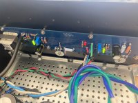
ITS ALIVE!!!! Q3 and Q4 were correct. Replaced D1 with green LED and ensured correct polarity. Q3 and Q4 were correct but noticed poor solder joint on backside for Q3 but just decided to reflow the entire board. Reinstalled and started to get readings at R2. Burning in and biasing now. So happy and excited!! Late now here so can't really test and turn it up. Can't wait to get home from work tomorrow to enjoy and continue this journey. Thanks Anand for the help. Also to Papa for the design, 6L6, Pico, ZM and so many others who have posted and shared their troubles, pics, and solutions. All was so helpful and critical in my learning and building process. I'm so hooked. Love this forum. Waynes BA 2018 is next in the near future.
Attachments
Thank you Anand!
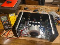
BTW, my power supply provides +26.2 V and -26.2 V to the board and I supplied it to one channel only. I successfully measured and set P2 bias of this channel (500 mV across R2) and "minimized" the offset to -430 mV measuring across the speaker outputs . . . could not get it to zero, even after allowing the heatsink to warm up after 30 minutes at the correct bias.
Then I moved to the other channel by providing power to it separately. A few seconds after connecting power, the R4 resistor ended up smoking and I immediately unplugged the power source. I measured the resistance of R4 and found it to be 15 ohms. I then turned the power on again to measure voltage across R4 and found it to be 9.4 volts. After a few seconds it started smoking again. Clearly there is a problem. I inspected the board and did not find any obvious issues (to a noob).
BTW, the boards that I received as part of the kit were not mirror images of each other and clearly had minor differences in the placement of the components, likely due to an update in the mapping of the same circuit at 2 differing dates.
Thoughts? Suggestions?
Rolf,
You have 1 problem on one channel (unable to reduce offset) and another problem on the other channel (could be a multitude of things).
I suggest you first show us detailed photos of how you have each of the channels wired up along with detailed photos of the specific boards themselves, i.e. Channel A/B of F6 PCB, power supply board(s), softstart circuit, chassis ground, etc....
You can't always reliably measure a resistor while in circuit, you have to desolder at least 1 end btw. That being said, we can get to the R4 issue a little later:
Check that none of the 3 pins on each of your MOSFETS has a connection to ground or to the chassis. They shouldn't. Make sure that the MOSFETS are electrically isolated from the heatsink. Sometimes metal burs from the heatsink or from the back of the MOSFET pierce through the insulation pad and short the MOSFET to the heatsink. The back of the MOSFET is a live part (it is connected to the drain pin), so insulating it is vitally important:
Building: Amp Boards on Heat Sinks
Check that Q3 is a 2SK170 (or equivalent) and that Q4 is a 2SJ74 (or equivalent) on each of the boards. Like you said, they are physically on slightly different locations.
I would strongly suggest either a dim bulb tester or variac before you consider turning the unit back on.
I would also strongly suggest that you have it fused (in the IEC socket) and also that you have proven beyond a reasonable doubt that you have a good chassis ground connection and a CL-60 thermistor going from the power supply ground to chassis ground. Then a wire should run from the chassis ground to earth ground on the IEC ground terminal. I like minimum 18AWG wires from the chassis ground to the IEC ground terminal, and typically I try 14 AWG or 16 AWG.
We should probably first work on the channel that doesn't have a smoking R4, i.e. the channel where you can't reduce the offset. You want to check what the voltages are across each of the zeners, Z1 and Z2. You also want to check what the voltages are on the MOSFETS particularly from gate to source (outer pins of IRFP 240). They should be around 4 ish volts.
Best,
Anand.
P.S. Courtesy to flohmann who wrote the Aleph J Build Guide for Noobs. This should be required reading for anyone who is going on a conquest to build Pass amplifiers.
You have 1 problem on one channel (unable to reduce offset) and another problem on the other channel (could be a multitude of things).
I suggest you first show us detailed photos of how you have each of the channels wired up along with detailed photos of the specific boards themselves, i.e. Channel A/B of F6 PCB, power supply board(s), softstart circuit, chassis ground, etc....
You can't always reliably measure a resistor while in circuit, you have to desolder at least 1 end btw. That being said, we can get to the R4 issue a little later:
Check that none of the 3 pins on each of your MOSFETS has a connection to ground or to the chassis. They shouldn't. Make sure that the MOSFETS are electrically isolated from the heatsink. Sometimes metal burs from the heatsink or from the back of the MOSFET pierce through the insulation pad and short the MOSFET to the heatsink. The back of the MOSFET is a live part (it is connected to the drain pin), so insulating it is vitally important:
Building: Amp Boards on Heat Sinks
Check that Q3 is a 2SK170 (or equivalent) and that Q4 is a 2SJ74 (or equivalent) on each of the boards. Like you said, they are physically on slightly different locations.
I would strongly suggest either a dim bulb tester or variac before you consider turning the unit back on.
I would also strongly suggest that you have it fused (in the IEC socket) and also that you have proven beyond a reasonable doubt that you have a good chassis ground connection and a CL-60 thermistor going from the power supply ground to chassis ground. Then a wire should run from the chassis ground to earth ground on the IEC ground terminal. I like minimum 18AWG wires from the chassis ground to the IEC ground terminal, and typically I try 14 AWG or 16 AWG.
We should probably first work on the channel that doesn't have a smoking R4
, i.e. the channel where you can't reduce the offset. You want to check what the voltages are across each of the zeners, Z1 and Z2. You also want to check what the voltages are on the MOSFETS particularly from gate to source (outer pins of IRFP 240). They should be around 4 ish volts. Best,
Anand.
P.S. Courtesy to flohmann
who wrote the Aleph J Build Guide for Noobs. This should be required reading for anyone who is going on a conquest to build Pass amplifiers.
Last edited:
- Home
- Amplifiers
- Pass Labs
- F6 Illustrated Build Guide