Official DUT schematic for N&P Vfet's Sit's ?
@ Mr Pass and Diyers
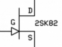
Any chance to have official schematic DUT vgs circuits for 2SK | 2SJ Sony Vfet's ?
I know is basic stuff for many people but help me avoid errors or make smoke poofff be highly apprecciated.
It was presented for mosfet's with psu, resistor and multimeter for n & p channel.
Any circuits ?
?
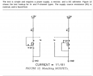
Since 19V is a common switching supply for laptops and is the same voltage
as the Vds in the amplifier, use that as the voltage and find the Vgs which
gives you 0.50 Amp current. It will generally be in the range of 6 to 11 volts.
So what's our procedure for measuring Vgs going to be so we can compare results?
Thanks,
So I assume we are really then grading on a pair that would take the same - bias voltage to get .50A @ 19v?
@ Mr Pass and Diyers
Any chance to have official schematic DUT vgs circuits for 2SK | 2SJ Sony Vfet's ?
I know is basic stuff for many people but help me avoid errors or make smoke poofff be highly apprecciated.
It was presented for mosfet's with psu, resistor and multimeter for n & p channel.
Any circuits
?Attachments
Why 500Hz for the measurements in this article instead of your usual standard of 1khz ?
Makes for a nicely framed scope shot.
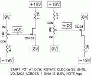
Here is an example test setup
Thanks Papa Diy Cool
Kind regards


if only this amp designed with common source mode.
which the original vfet character will be appear. (in my opinion)
^.^
All depends in the G-S transference curve.
Until today I like to know this trace.
I looked for long time.
I think the Common Drain or follower is transparent with only management in current.
I knew or I learnt (by assertive or wrong mind) that all the benefices became from the front end circuit.
Please with patience if is possible for the big monster pope open mind that read this thread if is true or fake, or more explain if anybody can show any.
Best Regards
Here is an example test setup
@ Mr Pass and Diyers
Ready for Vgs tests
") Sony's are on heatsink with mica & "polar snow"
Sony's are on heatsink with mica & "polar snow"I collected all parts after schematic and see parameters this evening.
Ccw direction on trimmer show me now 0 R it is ok like start point ? Yup ?
Thanks Mr Rothacher for useful Vfet pictures who help avoid mistakes

Greetings
Attachments
Maybe a quick check with the multimeter to verify actual resistance set by the trimmer?
Yes i have minimal 0 ohm resistance on trimmer
but maybe we need 10Kohm ? That question :
i know is better to ask and don't cry after rare diamond
have burn or something
 Thanks Have Fun
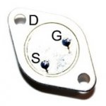
I just noticed that one of the 2SK82 I got to make the single pair version reads JF-33,as compared to KE-33 2SK82s that everone has.
I have no equipment immediately on hand to measure not even a cheap multimeter,but going just by looks,the printing is different compared to the rest of the VFETs, the case is matte,as opposed to the shinier cases of the others and a slight difference in can curvature. Is anything amiss?
I ask because of this-
2SK82 being unobtainum now,will there be any issues in getting this part to work?
I have no equipment immediately on hand to measure not even a cheap multimeter,but going just by looks,the printing is different compared to the rest of the VFETs, the case is matte,as opposed to the shinier cases of the others and a slight difference in can curvature. Is anything amiss?
I ask because of this-
any idea what JA-33 mean?
@Luke:
Is the Bath of production.
2SK82 being unobtainum now,will there be any issues in getting this part to work?
- Home
- Amplifiers
- Pass Labs
- Sony VFET Amplifier Part 2