I have previously expressed my admiration for Mike's effort by email, but it
is appropriate that I do so in public.
A corollary lesson here is that when you lay out a schematic clearly and then
make the pc board layout look like it as much as possible, everyone's job is
made very much easier.

is appropriate that I do so in public.
A corollary lesson here is that when you lay out a schematic clearly and then
make the pc board layout look like it as much as possible, everyone's job is
made very much easier.
I have previously expressed my admiration for Mike's effort by email, but it
is appropriate that I do so in public.
A corollary lesson here is that when you lay out a schematic clearly and then
make the pc board layout look like it as much as possible, everyone's job is
made very much easier.
Often the circuit will work better that way, too.
I have previously expressed my admiration for Mike's effort by email, but it
is appropriate that I do so in public.
A corollary lesson here is that when you lay out a schematic clearly and then
make the pc board layout look like it as much as possible, everyone's job is
made very much easier.
To Papa and those who have read (and even responded) to this thread:
Thank you....
I appreciate your interest and comments very much. It feels good to share something with you all from whom I have learned so much.
It's just plain 1/16" thick phenolic or fiberglass with no copper, and a grid of small holes all over the surface. Here's a sample:
22-516: GC ELECTRONICS: Electronic Design
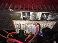
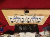
Here are some examples of construction using this type of board . The circuits pictured were built on a tenth inch grid drilled fiberglass board using gold plated stake pins for the connections to the outside world. The excellent layout from Papa made this board a quick and easy one to build. The board layout was photocopied to scale, glued onto the breadboard in alignment with the grid of holes, and components were inserted through the print. Most wiring connections were made by wrapping one component lead around the next and soldering them together. Where leads weren't long enough to touch, buss wire was used to make the connection. Where Papa placed traces on the top of his PC board I ran insulated wire on the bottom of the board. I would have used the excellent PC boards from the DIYAudio store, but I can never catch them in stock!
Attachments
Last edited:
Here are some examples of construction using this type of board . The circuits pictured were built on a tenth inch grid drilled fiberglass board using gold plated stake pins for the connections to the outside world. The excellent layout from Papa made this board a quick and easy one to build. The board layout was photocopied to scale, glued onto the breadboard in alignment with the grid of holes, and components were inserted through the print. Most wiring connections were made by wrapping one component lead around the next and soldering them together. Where leads weren't long enough to touch, buss wire was used to make the connection. Where Papa placed traces on the top of his PC board I ran insulated wire on the bottom of the board. I would have used the excellent PC boards from the DIYAudio store, but I can never catch them in stock!
Very nice work. I'd watch out for really hot components like the large resistors near the paper, though.
Hi Mike
I was guided by your thread and try assembly mono amp
8 watts Hiraga with old school point to point technique on tag boards.
Always admire Papa for D-Lite like stone soup amplifier
and L'Amp with Sony Vfets by Mr Rothacher.
My realisation is more spagetti to spagetti bit less . to .
Just experimentation Work at first power up !
Your thread inspired me to do this
i have good time last evening ,
and try more in near future with Zen's topologys
Thanks Mike


Hope next time i do with elegant tourrets boards like this:
How To Build a Turret Board Part 2: Swage Fitting - YouTube
Greetings
I was guided by your thread and try assembly mono amp
8 watts Hiraga with old school point to point technique on tag boards.
Always admire Papa for D-Lite like stone soup amplifier
and L'Amp with Sony Vfets by Mr Rothacher.
My realisation is more spagetti to spagetti bit less . to .
Just experimentation
Work at first power up !Your thread inspired me to do this
i have good time last evening ,
and try more in near future with Zen's topologys
Thanks Mike
Hope next time i do with elegant tourrets boards like this:
How To Build a Turret Board Part 2: Swage Fitting - YouTube
Greetings
Last edited:
Hi Mike
I was guided by your prototype and try assembly mono amp
8 watts Hiraga with old school point to point technique on tag boards.
Always admire Papa for De-Lite stone soup amplifier
and Mr Rothacher for L'Amp with Vfet´s.
My realisation is more spagetti to spagetti bit less . to .
Just experimentation
Your thread inspired me to do this
i have good time last evening ,
and try more in near future with Zen's topologys
Thanks Mike
Hope next time be with elegant tourrets boards like this:
How To Build a Turret Board Part 2: Swage Fitting - YouTube
Greetings
Photos
Attachments
Soundhappy
Nice job! Thank you for sending photos. There are similar terminal boards made that have smaller and closer together connections. Also things like the Jfets can be soldered into the holes under the bigger loops using adjacent terminals so as to put less stress on the part.
Very nice board... I bet it sounds fantastic!
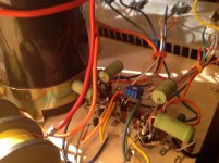
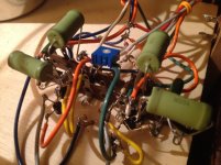
Here is one my son did recently ( with me looking over his shoulder of course). Notice the gate stopper resistors are attached directly to the gate lead of the mosfets. This is necessary to prevent instability. It is a pair of Papa's Complementary Zen amps.
Attachments
Last edited:
Soundhappy
Nice job! Thank you for sending photos. There are similar terminal boards made that have smaller and closer together connections. Also things like the Jfets can be soldered into the holes under the bigger loops using adjacent terminals so as to put less stress on the part.
Very nice board... I bet it sounds fantastic!
Hi Mike
Thanks for compliments and councils.
I like your old school technique : visual and directly on schematic wiring.
Stuffed pcb´s is less funny. After two days of music sessions
with 8 watt Hiraga like Papa classe A amp´s
if fantastic sound at input = fantastic sound at output
Fast transparent sounding and can surprise in good way
PSU have 500 000uF filter caps for mono and choke L too.
Your Son boards is the great ones very clear, i imagine it was
very enjoyable fun diy & make sound with complementary amplifier.
Have a nice day
Kindly regards
Soundhappy
Thank you...
I am happy that you have been inspired to build some circuits and listen to them. There is nothing quite like turning an amplifier and listening for the first time.
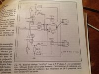
The Zen Complemetary circuit is particular about the power supply. We now need to build one like Papa presents in his excellent write-up. Sorry to all about the upside down picture for this amp. I wish I knew what I did to invert it and how to make it upright again. I am anxious to hear the amplifier. I also need to get larger heat sinks for the output devices. We just used spare parts from old amplifier equipment for the initial trial of the circuit. Keep up the good work!
I can't agree with Nelson's comment - schematics are meant to be read for circuit comprehension - not reflect physical layout
for electoral function/performance you never want +/- power entering your circuit from opposite edges, making large loop area with gnd
parts location diagrams are given for assembly and debugging
in fact sometimes point-to-point prototyping can be improved by using a PCB layout tool for the circuit, using the rubber banding tool to optimize parts placement and orientation to reduce high current loop areas, shorten sensitive nodes
I can't agree with Nelson's comment - schematics are meant to be read for circuit comprehension - not reflect physical layout
for electoral function/performance you never want +/- power entering your circuit from opposite edges, making large loop area with gnd
parts location diagrams are given for assembly and debugging
in fact sometimes point-to-point prototyping can be improved by using a PCB layout tool for the circuit, using the rubber banding tool to optimize parts placement and orientation to reduce high current loop areas, shorten sensitive nodes
JCX
What tool do you use that allows the "rubber banding" to be done? I do something similar manually, (using a PC based graphics program) but it would be great to have a tool to make it easier.
- Status
- This old topic is closed. If you want to reopen this topic, contact a moderator using the "Report Post" button.
- Home
- Amplifiers
- Pass Labs
- Old School Prototyping