I had no problem adjusting DC offset to zero. My concern is the difference in bias from P channel to N channel,
Sorry, must have misunderstood. I thought you had problems getting it to dero between the two output terminals.
Good luck! Should be two powerful amps!
Joe,
Somehow it seems your output devices are "on". Can you please confirm P1 and P2 settings by measuring the resistance across the R5 and R6 resistors (with power off).
They should be just a few ohms. And as Elwood suggested, please check for
proper placements of parts since you've replaced some, to also check for shorts.
Dennis
Good morning gang, Dennis and Elwood I will have to hang my head in embarrassment today. I changed all my source resistors when the MOSFETS smoked. Well......I overlooked installing R14. I soldered in the 47.5K resistor and I am now in the bias setting stages. Thank you guys so much for stepping in and assisting.
I have a quick question about bias. After I got my left channel up and running, I started to bias it. I brought it up slow letting it cook with the cover on. I now have it amp up and running at about 330mv’s on the P & N boards with dc offset almost 0 volts. I’m going to leave this here for a few days. I spoke with (6L6) Jim and he said the P & N boards bias may not be exactly identical but I didn’t ask how much of a difference is acceptable. My right channel has been set since last week so it’s biased at 350mv’s. I have roughly 20mv difference between the P & N boards with bias set at 350mv and dc offset almost zero. Is this acceptable or is there something I should look for?
I sent you tightly matched Ns and tightly matched Ps. I also sent the closest matches I had between Ps and Ns even though it's not critical ... jusssssst in case. ") Put 4V in front of the markings on the back, and those were my measurements.
Put 4V in front of the markings on the back, and those were my measurements.
Are you talking about right channel being at 350mV and left channel being at 330mV both N and P. Or are you talking about N on left being 330mV and P on left being 350mV? Both channels with nulled offset.
For clarity - What's your VDC for below:
Across TP 2 and 3 for N side - Left
Across TP 2 and 3 for P side - Left
Offset - Left
Across TP 2 and 3 for N side - Right
Across TP 2 and 3 for P side - Right
Offset - Right
I think you have a working F5T ... nicely done!
Put 4V in front of the markings on the back, and those were my measurements. Are you talking about right channel being at 350mV and left channel being at 330mV both N and P. Or are you talking about N on left being 330mV and P on left being 350mV? Both channels with nulled offset.
For clarity - What's your VDC for below:
Across TP 2 and 3 for N side - Left
Across TP 2 and 3 for P side - Left
Offset - Left
Across TP 2 and 3 for N side - Right
Across TP 2 and 3 for P side - Right
Offset - Right
I think you have a working F5T ... nicely done!
Last edited:
Patrick thanks for giving input. I’ll check in the AM, we’re on our way out for the night but the channel with your parts isn’t the issue.
Waits sec, I have this info
Right channel N= 349mv
Right channel P= 329mv
Right channel Offset = 2mv
Left channel N= 332mv
Left channel P= 332mv
Left channel offset -3mv
Waits sec, I have this info
Right channel N= 349mv
Right channel P= 329mv
Right channel Offset = 2mv
Left channel N= 332mv
Left channel P= 332mv
Left channel offset -3mv
Last edited:
Kinda hopin' mine are in the left channel.
Either way... I think you have a working F5T within the norms. I think I read somewhere that up to 50mV of difference between Ns and Ps on the same channel is OK. I had that in my notes when I was pondering building one. Sadly, I can't find the exact reference. I should really put links in my notes.
Someone that's actually built one should really chime in to confirm, but I might bring the left up to ~340mV and call 'er a done deal.
Hi Dirk -
You know this circuit very well. I am still learning. Could you take a look at the right channel in post #886, please? I think it's absolutely fine with ~20mV difference between N and P with offset nulled, but I could never find my exact reference to be certain. Intuitively this makes sense to me that N and P may have slightly different Ids at same gate voltage unless you specifically choose matches between N and P like for the left channel.
The difference between N and P (I think) is what nulling DC offset compensates for (I think).
However, just b/c I think it (don't know it) does not mean it's correct or that someone else should follow my advice.
Thanks Dirk and Patrick. I do have another concern this morning. I shut the amp down last night around midnight or so. So I thought today would be the day I out it on a scope and see what it looks like and then play it on some test speakers. Before I connected speakers to it I thought to see what things looked like in the morning and this is what I had. On my left channel which is the most stable of the 2, at power up my bias initially shot up to 442mv & 438mv with 128mv offset. Within seconds they all started to come down and after a minute or so the bias was where I had it set last night but my offset is hanging around -38/40mv. The right channel was pretty much the same thing or close jumping up to 407mv/387mv with offset at 108mv. Again these started to drop within seconds and within several minutes the bias was close to where I had it set but again the bias is around -50mv.
Another question I have about the right channel that I’ve had since I’ve got it running is the bias and offset are constantly fluctuating. The left channel is pretty stable within a couple of mv’s but the right channel is all over the board. It never sits in one place too long and I will see fluctuations from a couple mv’s to 30mv’s up up down then when it hits that high or low point, it immediately adjust back the other way. This affects offset respectively. Could this be caused from the thermistors on the output boards? I have them mounted so the tip is touching the casing of the MOSFETS. I think there was some conversation between Charles and Patrick in regards to some 4.7k thermistors with an eyehole for mounting which I actually ordered. They just haven’t arrived yet. Any thought on all the above? Should I re-adjust the bias or let it heat up totally and see where it ends up?
Another question I have about the right channel that I’ve had since I’ve got it running is the bias and offset are constantly fluctuating. The left channel is pretty stable within a couple of mv’s but the right channel is all over the board. It never sits in one place too long and I will see fluctuations from a couple mv’s to 30mv’s up up down then when it hits that high or low point, it immediately adjust back the other way. This affects offset respectively. Could this be caused from the thermistors on the output boards? I have them mounted so the tip is touching the casing of the MOSFETS. I think there was some conversation between Charles and Patrick in regards to some 4.7k thermistors with an eyehole for mounting which I actually ordered. They just haven’t arrived yet. Any thought on all the above? Should I re-adjust the bias or let it heat up totally and see where it ends up?
Last edited:
I have no experience with the F5 Turbo but I think to be sure, one should
measure the voltages across all 4 sets of source
resistors. (F5 turbo V2 schematics on page 9, at R17, R19, R21, R23):
https://firstwatt.com/pdf/art_f5_turbo.pdf
You want the dc offset to be close to zero. Assuming the source resistors
are closely matched and the diodes aren't 'on' the sum of the voltages
of the two polarities should also be close.
But this means if one voltage measurement is low, the other one in
the same polarity will be higher.
I think the diodes creates a complication here and you want to make
sure the mosfets for each polarity are sufficiently well-matched so that
at your desired bias level, none of the source resistor measurements
get close to the 0.4 volt danger zone.
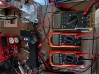
Hi Dennis, thank you for the info. This is what I have but unfortunately am not sure what is means. Looks like there may be some averaging going on?
Right channel F5T
N board- R21=345mv R22=346mv R23=295mv R24=313mv
P board- R17=326mv R18=322mv R19=323mv R22=315
Test pins N=348 P=324
Left channel F5T
N board- R21=342mv R22=343mv R23=354mv R24=350mv
P board- R17=345mv R18=344mv R19=343mv R22=347
Test pins N=347 P=346
Right channel F5T
N board- R21=345mv R22=346mv R23=295mv R24=313mv
P board- R17=326mv R18=322mv R19=323mv R22=315
Test pins N=348 P=324
Left channel F5T
N board- R21=342mv R22=343mv R23=354mv R24=350mv
P board- R17=345mv R18=344mv R19=343mv R22=347
Test pins N=347 P=346
- Home
- Amplifiers
- Pass Labs
- F5Turbo Illustrated Build Guide