
Thanks Zen Mod. Understood.in layman terms, sound is polite with lesser details, used in position as that
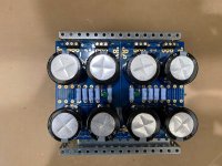
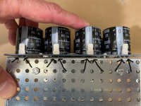
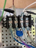
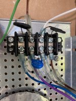
I appear to have blown something when testing the PS. I hope someone can give me a little guidance. I am building Aleph J monoblocks with the DIYAudio universal power supply. I wired up the power supply for the first block. Using the dim bulb tester, the bulb did not dim and I turned everything off. In looking at the PSU board, I noticed that I had it set up such that all the power inputs to the board were shorted. I managed to inadvertently do that by placing the board on top of a riser panel set up over the transformer. The first picture shows a top view of how I thought I had it set up. Unfortunately, i had removed and replaced the PS pcb several times in wiring it up and inadvertently placed it not in the middle of the top riser plate, but on the edge, effectively connecting all power inputs together (see second picture).
After observing my incredibly stupid placement of the pcb, I moved it where it should have been (as shown in first picture) and tried again. This time the bulb dimmed then went out. I was reading no voltage on the outputs of the universal power supply board. I unhooked the power supply board and tested just the secondary coils of the transformer. The bulb did not light, but each coil measured 20 volts ac. (The transformer is supposedly 18-18 volts.) I then tried measuring the output of the bridges. Before powering on, my volt meter displayed some milli voltage on the bridges, when I turned on the power, the bulb did not light and the meter immediately went to OL. I tried wiring in the second set of bridges, but got the same result. (I also changed the bulb in the dim bulb tester to no avail).
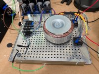
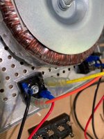
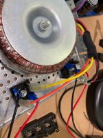
My next step would be to buy 4 new bridges and try again. Does that seem like the correct next step? Also, is there some way to check the Universal Power Supply board to make sure I did not blow any of the capacitors? Should I also get a new ps pcb and capacitors etc? The final picture shows the transformer wired up after I removed the ps pcb and disconnected it from the bridges. Any help would be appreciated.
After observing my incredibly stupid placement of the pcb, I moved it where it should have been (as shown in first picture) and tried again. This time the bulb dimmed then went out. I was reading no voltage on the outputs of the universal power supply board. I unhooked the power supply board and tested just the secondary coils of the transformer. The bulb did not light, but each coil measured 20 volts ac. (The transformer is supposedly 18-18 volts.) I then tried measuring the output of the bridges. Before powering on, my volt meter displayed some milli voltage on the bridges, when I turned on the power, the bulb did not light and the meter immediately went to OL. I tried wiring in the second set of bridges, but got the same result. (I also changed the bulb in the dim bulb tester to no avail).
My next step would be to buy 4 new bridges and try again. Does that seem like the correct next step? Also, is there some way to check the Universal Power Supply board to make sure I did not blow any of the capacitors? Should I also get a new ps pcb and capacitors etc? The final picture shows the transformer wired up after I removed the ps pcb and disconnected it from the bridges. Any help would be appreciated.
Attachments
Your bridges may still be ok.
However it's impossible to assess your wiring based on your pictures. You need to post pictures that clearly show the connection of wires to the board, recitifers, transformer, AC power, CL60s., etc. Overhead shots of the complete circuit so that all of the wiring can be traced and verified.
The best way to build the power supply is to do it in stages and test each stage.
Connect the AC from input to CL60s and power transformer. With dim bulb tester in place, power up and measure the AC voltage at the transformer secondaries. If dim bulb tester is dim and there is AC voltage, that is good.
Next connect the secondaries to the rectifier bridges. Is there DC voltage at the output of the rectifier bridges? If yes, that is good.
Next connect rectifier outputs to the PS board and power up and check.
At all stages check and double check that your wiring and connections are correct. Make sure AC is connected to the AC input of the rectifier bridge and DC positive and negative out of the rectifier bridge are connected to the correct points on the PS board. When connecting the transformer secondaries to the bridges, check that you have paired the secondary wires correctly.
What voltage range was your meter set to? Or is it auto ranging?when I turned on the power, the bulb did not light and the meter immediately went to OL.
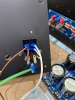
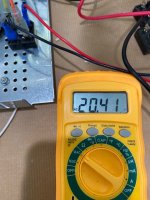
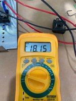
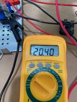
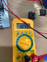
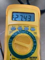
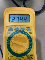
Thank you Ben Mah and KevinHeem. I have a feeling the OL resulted from my meter being out of range. Ben Mah, I have attached pictures showing my wiring (I intend to remove the shrink wrap from the legs of the CL60 as I understand they may get very hot - I will try the ceramic block that the Noob Guide shows). I tried measurements as you suggested. First, with the PS pcb unattached, I measured transformer secondaries - I got 20.4 ac. I then measured the output of the bridges - I got 18.19 and 18.15 dc. The bulb never lit. I then hooked up the ps pcb, the bulb lit and dimmed to nothing - I got 27.43 negative on one set of outputs and 27.41 positive on the other. I turned it off between measurements to relocate the test probes and when I turned it back on the bulb did not light but I got similar readings.
I am confused about the 18 volts out of the bridge and 27 volts out of the ps. Should I take those again?
Anyway it appears that it might be working, but I wonder why my dim bulb tester dims to nothing and then does not light. Any thoughts?
I am confused about the 18 volts out of the bridge and 27 volts out of the ps. Should I take those again?
Anyway it appears that it might be working, but I wonder why my dim bulb tester dims to nothing and then does not light. Any thoughts?
Attachments
-
 IMG_8289.jpg52.2 KB · Views: 61
 -
 IMG_8290.jpg83.4 KB · Views: 60
 -
 IMG_8291.jpg87.1 KB · Views: 64
 -
 IMG_8294.jpg73.2 KB · Views: 54
 -
 IMG_8295.jpg81 KB · Views: 57
 -
 IMG_8296.jpg71 KB · Views: 55
 -
 IMG_8298.jpg71.6 KB · Views: 53
 -
 IMG_8299.jpg53.2 KB · Views: 63
 -
 IMG_8300.jpg73.8 KB · Views: 62
 -
 IMG_8301.jpg71.5 KB · Views: 50
 -
 IMG_8305.jpg72.6 KB · Views: 51
 -
 IMG_8307.jpg63.5 KB · Views: 50
 -
 IMG_8308.jpg61 KB · Views: 59
When only the transformer is connected and when only the transformer and rectifiers are connected, there is no load connected so the bulb not lighting is correct, as there is no load to draw current. So it is working properly.
The voltages look good too. With the rectifiers connected, the voltages are lower because there are no capacitors.
Then with the capacitors in the circuit, they charge up and increase the DC voltage. The bulb lights up as current flows to charge the capacitors. Once the capacitors are charged, the current flow stops and the bulb goes dark.
The voltage of 27V seems high but that will drop once the amplifier boards are connected and draw current from the power supply.
It looks like your power supply is working correctly.
Now when you connect the ampliifier boards, only connect one board at the beginning, and of course use the dim bulb tester. Only connect the second channel once you have the first channel working properly.
Last edited:
I'm using the schematic in post #1 of this threadI believe Zen Mod wanted you to check the power dissipated by the Jfets and Mosfets to make sure you are not exceeding their maximum safe operating values and risk destroying them.
So you need to know the voltage drop across/through them and the current through them to calculate the power dissipated. The voltage drop is measured from drain to source, so measure VDC with probes at drain and source. To determine the current measure the voltage drop across the Mosfet source resistor and use Ohm's Law to calculate the current. To determine the current through the Jfets, a similar measurement is also needed. There are resistor(s) in the Jfet circuit that can be used. A resistor or pot that is in series with the Jfets may be measured for voltage drop and knowing the resistance, the current can be calculated. Post your Aleph J schematic if in doubt.
I think Zen Mod is also concerned that the Jfets' maximum voltage is not exceeded. Jfets in general have a low maximum voltage Vds.
As Zen Mod mentioned, data sheets may be checked for maximum dissipation of the Mosfet/Jfet. The maximum dissipation is usually given at 25 degrees C, and derating is needed for actual operating temperature. If no derating chart is given, typically a factor of 4 or so is used.
So I've measured the Jfets with the amp powered at +24/-24V.
D to S voltage:
Q1A = 19.30 VDC
Q1B = 23.87 VDC
* Is it odd these voltages aren't closer to each other?
I'm going to just concentrate on calculating the dissipation for Q1B to see If I'm understanding the concept. So R8 (1K resistor) is in series with Q1B and the voltage reading is 8.39 VDC across that resistor.
I = 8.39V / 1000R so I = 8.39mA
23.87V x 8.39mA = 200 mW
The Data Sheet for a 2SJ74 lists Drain power dissipation at 400mA. So derating it for temperature means the Jfet should only dissipate 100mA?
I'm not sure my thinking is clear on any of this. Am I in the ballpark?
Edit: R8 is a 1K fixed resistor and there is no pot (as shown on the schematic) installed on my board.
Last edited:
Close.
Q1A and Q1B are paralleled. So the 8.39mA is split between Q1A and Q1B. It is possibly not equally divided but for a rough estimate assume it is. So the power dissipation is half of what you calculated.
The voltage drop across Q1A is less than across Q1B because R7 in series with Q1A also drops voltage. The voltage drop across Q1A+R7 equals the voltage drop across Q1B=23.87V.
So for a more precise calculation of power dissipation, using your measurements and if R7 is 1k, voltage drop across R7 is 23.87V-19.3V=4.57V. Current through Q1A and R7 = 4.57V/1000R=4.57mA. The rest of the 8.39mA goes through Q1B.
So Q1A power dissipation = 19.3Vx4.57mA=88mW
Q1B power dissipation = 23.87Vx(8.39mA-4.57mA)=91mW
Both are less than 100mW so should be safe.
Similar calculations may be done for the output Mosfets.
Is there a description or name for the arrangement of Q1A and Q1B. Other FW clones I've built have an article where Nelson walks through the circuit and explains how some of the active and passive components are used. This amp uses a different arrangement than the others I've built and there is no article explaining the circuit.
My observation too. Never did dare to ask why that is. I almost began to think I had ordered lateral MOSFETs insted of vertical, since the tempco seemed negative. But apparently this is normal for this circuit.I'm getting ready to measure the output Mofets and I've noticed it takes quite a long time for the bias (voltage arcoss R17...) to settle down. Also the voltage starts high and drifts down which seems different.
- Home
- Amplifiers
- Pass Labs
- Aleph J illustrated build guide