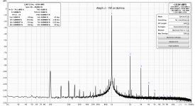
I made some distorsion measurements. Overall looks ok, I think (picture attached).
But I also measured the temperature on the drain pin on Q5 - got 150C. Not cool (pun intended...)! I suppose this mosfet runs on the limit of the junction temperature.
I know: "We are fearless amplifier builders. A little heat doesn't scare us at all." But I would not want solder to start melting. Should do something about it. No?
-Alvis
Attachments
Pass DIY Addict
Joined 2000
Paid Member
Those sticky pad seems to be very thick and also highly compressible. This makes it likely that you are getting inconsistent mounting pressure which can lead to inconsistent temperatures are you seeing. Also, not knowing exactly how matching is done for the store, you might want to verify their measurements. You can do this one step at a time.
My first suggestion is to ditch the sticky pads and use something proven/known for this purpose. I would recommend using Aluminum Oxide Ceramic with some thermal paste. Something like Aavid 4180G that you can find here:
https://www.mouser.com/ProductDetail/Aavid/4180G/?qs=%2Fha2pyFadui1fXtI3x%2FsVAEB0%252BomdHlMoIf3lcZu5sY%3D
These provide the best thermal transfer (more than three times better than the sticky pads you linked) and excellent electrical insulation. You can also find them on ebay, just search on "aluminum oxide ceramic" and order lots of them (because you'll likely build another amp later).
If you are seeing temps of 80c and up, you are likely to burn your mosfets in a very short period of time. I would recommend not powering up the amp until you have good/known thermal pads in place first. After replacing your thermal interface, remeasure things and we'll go from there. I'm thinking better thermal pads will probably solve your problem.
Last edited:
as Eric said - toss that sticky thingies, use whatever you find, but proven
either Alu Oxide or simple mica+goo, and you'll be good
btw. I have doubts in whatever you used for measurements of temperature - 150C at drain pin - sorta impossible - mosfet is looooong gone before reaching 150C at pin
change pads, then make all your measurements at source resistors; with some luck - it could happen that mosfets are matched , but their thermal interface wasn't
Thanks for your suggestion, Eric.
Mouser shipping costs to me are too high for small orders, but I found something similar (with even better thermal conductivity) on RS that delivers free in Lithuania. Hope that would also be fine:
SL-012-AL-20 | Thermal Interface Pad, Ceramic Aluminium Oxide, 20W/m*K, 23 x 20mm 2mm | RS Components
I could order the pads and would have them delivered in about a week.
And then, would any thermal paste be fine? I have some NTE303 (thermal conductivity, K factor, cal/cm2/°C/sec/cm - 0.001) and AGT-055 (heat-transfer coefficient at 0-50°C:0,88 W/m K). Would it be ok?
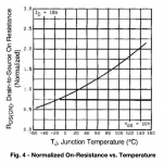
But can bad heat sinking explain the differences in voltages accross the power resistors? From the specs of IRFP240 I see that its Drain-to-Source On Resistance increases with increase of the Junction Temperature (see the pic.), so wouldn't the current through the mosfet and therefore the voltage on the resistor decrease, not increase when the mosfet is too hot? Just asking as I want to understand how it works (my understanding of the schematics is quite limited yet).
Edit: Thanks Zen Mod also. Hm... my mosfets are strong then. I measured with UNI-T UT50C thermal probe on the pin.
-Alvis
Mouser shipping costs to me are too high for small orders, but I found something similar (with even better thermal conductivity) on RS that delivers free in Lithuania. Hope that would also be fine:
SL-012-AL-20 | Thermal Interface Pad, Ceramic Aluminium Oxide, 20W/m*K, 23 x 20mm 2mm | RS Components
I could order the pads and would have them delivered in about a week.
And then, would any thermal paste be fine? I have some NTE303 (thermal conductivity, K factor, cal/cm2/°C/sec/cm - 0.001) and AGT-055 (heat-transfer coefficient at 0-50°C:0,88 W/m K). Would it be ok?
But can bad heat sinking explain the differences in voltages accross the power resistors? From the specs of IRFP240 I see that its Drain-to-Source On Resistance increases with increase of the Junction Temperature (see the pic.), so wouldn't the current through the mosfet and therefore the voltage on the resistor decrease, not increase when the mosfet is too hot? Just asking as I want to understand how it works (my understanding of the schematics is quite limited yet).
Edit: Thanks Zen Mod also. Hm... my mosfets are strong then. I measured with UNI-T UT50C thermal probe on the pin.
-Alvis
Attachments
Last edited:
Pass DIY Addict
Joined 2000
Paid Member
Those ceramic insulators are perfect! Just about any thermal paste will work well, both sides of the ceramic wafers need to be coated. This should produce more uniform temps when mounted to the sinks and, as you've noted, temps are directly related to resistance, so this should even things out. If you are still having trouble after replacing the insulators, we'll explore other options.
yup, and amplifier is not functional with those bad verticals ...........
use laterals, and OLG is much lower, then you'll ask how and what to change to improve wooly sound, which you'll have , if using it with even just a little more demanding speakers
laterals are for Mini Alephs, no brainer
use laterals, and OLG is much lower, then you'll ask how and what to change to improve wooly sound, which you'll have , if using it with even just a little more demanding speakers
laterals are for Mini Alephs, no brainer
While waiting for the replacement thermal interface pads, I have one more question. Minor thing, but would be interesting for me to understand this.
I noticed that when I switch the power off, the LED3 (on the positive rail) fades out immediatelly, but the other ones (LED2, on the negative rail) continue to glow for about half a minute fading out gradually. Is this usual with Aleph J?
I extended two of them to the front pannel (closest to it, naturally), and now when I switch the power off, the left one is immediatelly off, and the right one is not... These are blue LEDs, so quite bright overall. I used 100K resistors on these that are on the front pannel.
I will be able to rewire them when I take the boards off the heatsinks anyway, but strange.
-Alvis
Last edited:
Ok, thanks, Dennis. Fine then.
But on the purpose of learning, why this happens? What capacitor is discharging through the LED2? I am quite a beginner, so my understanding of the circuits is very limited. When looking at the schematics I would recon that C2 could be discharging via LED3 (but appareintly it's not). Cannot understand the effect on LED2
But on the purpose of learning, why this happens? What capacitor is discharging through the LED2? I am quite a beginner, so my understanding of the circuits is very limited. When looking at the schematics I would recon that C2 could be discharging via LED3 (but appareintly it's not). Cannot understand the effect on LED2
layout okay?
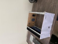
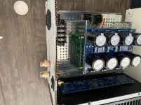
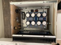
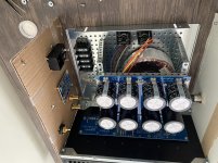
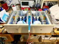
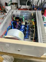
I am in the middle of putting together monoblocks. The chassis will be built around the diyaudiostore 4U 300mm heatsinks. I also am using a baseplate designed for the Galaxy chassis. I am trying to keep each monoblock relatively small. So far I have created a mock chassis measuring 280 X 300. In addition to the Aleph J pcb and the power supply, I will be using Mark Johnson's low power ac on off switch pcb and Tom Christiansen's Guardian-86 pcb for speaker protection. I will also be adding two fans under the heatsinks blowing up to keep things cool (my speakers are 4 Ohm).
I have attached photos of my layout. Could someone let me know if I am doing this correctly or not? If worse comes to worst, I could make the chassis a little wider (I have not had the back, front, side, top or bottom panels fabricated yet).
I would appreciate any help anyone can give me.
Thank you,
Jazzzman
Attachments
-
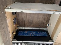 A Chasis mockup interior heatsink view.jpg1,013 KB · Views: 296
 -
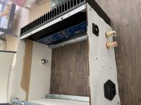 C Chassis mockup backplate view.jpg977.5 KB · Views: 296
 -
 E Chassis mockup front.jpg830.8 KB · Views: 237
 -
 G config back aerial view (lv switch pcb).jpg1,023.7 KB · Views: 234
 -
 K config from above with side panel.jpg1,014.9 KB · Views: 229
 -
 Q config rhs view.jpg1,011.2 KB · Views: 156
Lookin good. I built AJ as single 3U 400 chassis (would like to revisit as monoblocks). Here's scratch built M2X monos with very similar dimensions to what you are doing, food for thought, my widths were 9.5" interior. DIY PSU with attached diode bridge. Later I also added Mark's power control boards to the back wall (highly recommended).
What about flipping your grid plate so you can maximize the interior width? Might not be possible in your configuration. Also, I might recommend putting the transfo in one of the antek steel cans. I think they help—and look at what an L bracket arrangement might do for you—just to see.
What about flipping your grid plate so you can maximize the interior width? Might not be possible in your configuration. Also, I might recommend putting the transfo in one of the antek steel cans. I think they help—and look at what an L bracket arrangement might do for you—just to see.
Attachments
- Home
- Amplifiers
- Pass Labs
- Aleph J illustrated build guide