I proposed in a past post of this thread the attached schematic in the event additional voltage gain was needed in diyF6. I already bought the PCBs from the DIYAudio store. I hope the schematic is useful for DIYers. One pending question hung: Where's one inject overall loop feedback in it?
Brgds.
why not just like the f6 unbuffered - ie R2 resistor between tx primary and gnd and R1 from o/p (F6 Unbuffered schematic) ? The Ba-3 front end doesn't look like it needs much in the way of feedback.... actually come to think of it you have followers in the op stage so you might be able to escape overall fb altogether imo.
Here is my P2P F6. Not exactly totally safe construction.
I biased at what I think if 1.5A.
Measuring V across resistors in standard Pass supply.
1.5 x .(4x.47R) in power supply = .176
No big sound evaluation yet, just one mono CHR-70 running no baffle.
I have ordered The Cree SIC Mosfets, and will modify this to use them adding more LED's.
Because I used a choke filter to take advantage of my 30-0-30 transformers I just lifted the lead at Q1's drain and inserted the DMM in line. Worked well with the PTP.
Looking forward to experimenting with the harmonics.
This is a fun amp! and it sounds great too
Best
Bob
Especially complimentary followers.

.... not me , Bubba .
Mighty ZM hate any sort of authority

why not just like the f6 unbuffered - ie R2 resistor between tx primary and gnd and R1 from o/p (F6 Unbuffered schematic) ? The Ba-3 front end doesn't look like it needs much in the way of feedback.... actually come to think of it you have followers in the op stage so you might be able to escape overall fb altogether imo.
Feedback in certain Pass FET circuits [ACA, F5 and F6] is like Schade Feedback in tube circuits with possible and welcome good side effects. Any modification of F6 must [imo] have the following prerequisites:
- An output stage [e.g. with MOSFETs and degen] like that with R100A. Either case is a current source amp prior to loop feedback with intrinsic pentode-like output characteristics. Complementary symmetry is doable but will not cut it because it is intrinsically a voltage source amp.
- Overall loop feedback to a summing [voltage substracting] junction like the novel one in F6. This is the special Pass Feedback. It carries the high probability of reorganizing the intrinsic pentode-like characteristics [open loop] to triode-like characteristics in the resultant F6 voltage source amp [Pass Feedback].
Brgds
More Cree stuff, I can't give it up!!
Again with the Cree stuff. CMF10120D
So I know it will turn on fully at lower VGS, however, in looking to tell if the tempco allows one to run without source degeneration, I can across this at the end of the speadsheet. Any comments? I am beginning to think an IRF240 might be better.
There are two key characteristics that need to be kept in mind when applying the
SiC DMOSFETs; modest transconductance and no turn-off tail. The modest transconductance requires that VGS
needs to be 20V to optimize performance. This can
be seen the Output and Transfer Characteristics shown in Figures 1-3. The modest
transconductance also affects the transition where the device behaves as a voltage
controlled resistance to where it behaves as a voltage controlled current source
as a function of VDS
. The result is that the transition occurs over higher values of
VDS
than is usually experienced with Si MOSFETs and IGBTs. This might affect the
operation anti-desaturation circuits, especially if the circuit takes advantage of the
device entering the constant current region at low values of forward voltage.
The modest transconductance needs to be carefully considered in the design of the
gate drive circuit. The first obvious requirement is that the gate driver be capable
of a 22V (or higher) swing. The recommended on state VGS
is +20V and the recommended off state VGS
is between -2V to -5V. Please carefully note that although
the gate voltage swing is higher than typical silicon MOSFETs and IGBTs, the total gate charge of the SiC DMOSFET is considerably lower. In fact, the product of
gate voltage swing and gate charge for the SiC DMOSFET is lower than comparable
silicon devices. The gate voltage must have a fast dV/dt to achieve fast switching
times which indicates that a very low impedance driver is necessary. Lastly, the
fidelity of the gate drive pulse must be carefully controlled. The nominal threshold
voltage is 2.3V and the device is not fully on (dVDS
/dt ≈ 0) until the VGS
is above
16V. This is a noticeably wider range than what is typically experienced with silicon MOSFETs and IGBTs. The net result of this is that the SiC DMOSFET has a
somewhat lower ‘noise margin’.
Again with the Cree stuff. CMF10120D
To do this, I would guess that the LED's would need to be a string of 5 or so, to allow for its 20V+ gate charge. We are assuming it also has less distortion than IRF240 and similiar sound to R100. Won't know until you try.
So I know it will turn on fully at lower VGS, however, in looking to tell if the tempco allows one to run without source degeneration, I can across this at the end of the speadsheet. Any comments? I am beginning to think an IRF240 might be better.
There are two key characteristics that need to be kept in mind when applying the
SiC DMOSFETs; modest transconductance and no turn-off tail. The modest transconductance requires that VGS
needs to be 20V to optimize performance. This can
be seen the Output and Transfer Characteristics shown in Figures 1-3. The modest
transconductance also affects the transition where the device behaves as a voltage
controlled resistance to where it behaves as a voltage controlled current source
as a function of VDS
. The result is that the transition occurs over higher values of
VDS
than is usually experienced with Si MOSFETs and IGBTs. This might affect the
operation anti-desaturation circuits, especially if the circuit takes advantage of the
device entering the constant current region at low values of forward voltage.
The modest transconductance needs to be carefully considered in the design of the
gate drive circuit. The first obvious requirement is that the gate driver be capable
of a 22V (or higher) swing. The recommended on state VGS
is +20V and the recommended off state VGS
is between -2V to -5V. Please carefully note that although
the gate voltage swing is higher than typical silicon MOSFETs and IGBTs, the total gate charge of the SiC DMOSFET is considerably lower. In fact, the product of
gate voltage swing and gate charge for the SiC DMOSFET is lower than comparable
silicon devices. The gate voltage must have a fast dV/dt to achieve fast switching
times which indicates that a very low impedance driver is necessary. Lastly, the
fidelity of the gate drive pulse must be carefully controlled. The nominal threshold
voltage is 2.3V and the device is not fully on (dVDS
/dt ≈ 0) until the VGS
is above
16V. This is a noticeably wider range than what is typically experienced with silicon MOSFETs and IGBTs. The net result of this is that the SiC DMOSFET has a
somewhat lower ‘noise margin’.
Again with the Cree stuff. CMF10120D
...
Looking at the CMF10120D datasheet, figure 3 suggests an undesirable temperature coefficient for use without degeneration and/or thermistors.
I haven't attempted to estimate the Beta (or Kappa) parameter from fig 1 and fig 2, but the transconductance looks to be approximately 1 at 1.5 amps Id. That would mean an F6 open-loop gain of only 16 with an 8 ohm load.
To me the CMF10120D doesn't look appropriate for the F6.
lhquam: kasey97 suggested in an earlier thread to use a step-up transformer to generate added open loop gain. Will it and/or a BA-3 gain front end help the solution with an IRFP240 output stage? Where and how will Mr. Pass find an open loop gain of 38 dB for the mod F6 like in original F6?Looking at the CMF10120D datasheet, figure 3 suggests an undesirable temperature coefficient for use without degeneration and/or thermistors.
I haven't attempted to estimate the Beta (or Kappa) parameter from fig 1 and fig 2, but the transconductance looks to be approximately 1 at 1.5 amps Id. That would mean an F6 open-loop gain of only 16 with an 8 ohm load.
To me thedoesn't look appropriate for the F6.
Has anybody heard the Cree parts?
I heard they sound Cree-py!
Seriously, I can't imagine Nelson hasn't auditioned everything currently available.
The attached schematic diyACAF6.pdf maybe a temporary solution for diyF6 using IRFP240s in the output stage:
- Use ACA for the output stage. This amp is highly acclaimed.
- Connect the secondary windings of the Jensen in series. The net winding is the input to 2SK170. This may double the open loop gain. Or, one may triple the open loop gain by connecting one of the two primary windings in series with the series-connected secondary windings; clearly if this electrically proper as I am not skilled in transformers. Note that I used the novel Pass Feedback summing junction twice; in the primary and secondary coils.
Attachments
A stand alone ACA has an open loop gain of 23 dB. Thus, it falls short of the specified 39 dB in F6; per Mr. Pass. IRFP240 may have higher distortion, lower Gm, and an added source degeneration required relative to R100A. We look forward to his simple solution and those of other DIYers' to attain an open loop voltage gain of 80. This race for a simple solution is on.Just look at post 2992 from Nelson.
He says how to.
I hope that Variac can keep the shelves of diyAudio Store stocked with the existing ACA PCBs and components. My proposed schematic may be tweaked to become the basis of a high power modified ACA; instead of a modified F6.
Brgds
Based on shematic in http://www.diyaudio.com/forums/pass-labs/216616-f6-amplifier-60.html#post3249226
Can I assume that P3+P4 will be normal 1/4-1/2 watt pots? Not certain at all being in line with Source degeneration resistors.
Also - do we still want to see a pot across the upper tranny pins 5 and 7?
I am stuck on this issue on my current layout.
Can I assume that P3+P4 will be normal 1/4-1/2 watt pots? Not certain at all being in line with Source degeneration resistors.
Also - do we still want to see a pot across the upper tranny pins 5 and 7?
I am stuck on this issue on my current layout.
Can I assume that P3+P4 will be normal 1/4-1/2 watt pots? Not certain at all being in line with Source degeneration resistors.
>>yup... Even assuming 10'amps thru rs, that means max 1 volt or so across rs ... Let's call it 2 to give us extra margin - gives us max dissipation in the pots of 4/10 = 0.4w so 0.5 w should be plenty. Guess 0.25w would be fine too...
Also - do we still want to see a pot across the upper tranny pins 5 and 7?
>> can't imagine why you'd need or want them since you've got the zen love pots across Rs already ...
I am stuck on this issue on my current layout.[/QUOTE]
I didn't see a lot of effect from the pot loading of the secondary windings and went for the pots across source resistors instead. There doesn't appear to be any significant ill effect from using small source resistors (like 0R1).
The cap on the input side was to reduce the high frequency rolloff at 20kHz. Without the cap, 20kHz is 0.5 dB down.
The cap on the input side was to reduce the high frequency rolloff at 20kHz. Without the cap, 20kHz is 0.5 dB down.
Ilquam noted that the pots across the secondaries did not do as much for him, but he had balanced the windings outputs with a cap on input side I believe. In doing this, I believe he pushed the adjustabillity to the output.
To determine the power dissipation of the Zen pots, use the following formula:
Zen_watts = (Rs*Ipeak)^2/R_Zen,
where Rs is the value of the source resistor, Ipeak is the peak current through Rs (usually 2*Ibias) add R_Zen is the reistance of the Zen pot.
Example: Zen_watts = (0R1*3A)^2/10R0 = .09 watts.
Zen_watts = (Rs*Ipeak)^2/R_Zen,
where Rs is the value of the source resistor, Ipeak is the peak current through Rs (usually 2*Ibias) add R_Zen is the reistance of the Zen pot.
Example: Zen_watts = (0R1*3A)^2/10R0 = .09 watts.
Based on shematic in http://www.diyaudio.com/forums/pass-labs/216616-f6-amplifier-60.html#post3249226
Can I assume that P3+P4 will be normal 1/4-1/2 watt pots? Not certain at all being in line with Source degeneration resistors.
Also - do we still want to see a pot across the upper tranny pins 5 and 7?
I am stuck on this issue on my current layout.
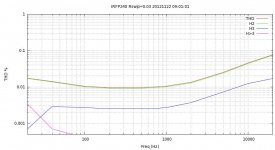
Here is an LTSpice simulation of the F6 using IRFP240 fets, and "tuning the Zen pot to keep the ratio H2/H3 approximately constant. I estimate the transconductance of the IRFP at 1.4A bias to be 3.5S.
This looks pretty good. I need to build it and see how it measures and sounds.
This looks pretty good. I need to build it and see how it measures and sounds.
Attachments
Rs=0R47 sounds about right for thermal stability. Any reason not to use one or more "Zen pots"?
I will suggest that you degenerate the IRFP240's with .47 ohms on the
DC bias portion and then connect the capacitor to the Source pin so that
it is not degenerated AC. I expect the distortion figure to be a little higher,
but no big deal.
- Home
- Amplifiers
- Pass Labs
- F6 Amplifier