Simulations of a circuit based on post #4540 http://www.diyaudio.com/forums/pass-labs/216616-f6-amplifier-454.html#post3527968 suggest that it would perform very well with NO FEEDBACK, having an open-loop gain of about 70 into 8 ohms and -3dB at 67kHz.
The artwork is finished and I intend to order PCBs tomorrow.
With your PCBs in my hands, I maybe able to expand the versatility of your circuit. Please see the attached picture of my hand-drawn circuit of it.
- Use the junction of the opposed drains of the cascoding transistors as COMMON or Ground
- Derive the power output port [Vo] at the junction of the two power supplies.
Attachments
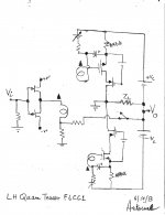
With your PCBs in my hands, I maybe able to expand the versatility of your circuit. Please see the attached picture of my hand-drawn circuit of it.
This new circuit has the performance attributes of the parent [source and drain currents are identical]; plus an intrinsic low impedance prior to applying negative feedback. Its enabled negative feedback is not Pass but the classical Black. Thus the amp is expected to have pentode-ish characteristics.
- Use the junction of the opposed drains of the cascoding transistors as COMMON or Ground
- Derive the power output port [Vo] at the junction of the two power supplies.
I suspect that the upper cascode fet is intended to be PMOS -- the arrow is wrong. The bottom coupling cap is backwards. The bottom secondary winding is backwards.
Interesting idea. When you start to float the power supplies, the circlotron topologies come to mind. Here is my analysis of the proposal: Ignoring interwinding capacitances for the moment, I suspect that the two alternatives would be equivalent. When interwinding capacitances are considered, in your design the secondaries that an AC swing equal to Vout relative to the primary windings, which will generate 2nd harmonic distortion increasing with frequency. In my design, the secondary windings have very little AC modulation relative to the primary.
I suspect that the upper cascode fet is intended to be PMOS -- the arrow is wrong. The bottom coupling cap is backwards. The bottom secondary winding is backwards
Thanks for your post. My apology for my mistakes above. May I ask:
Thanks for your post. My apology for my mistakes above. May I ask:
- What are the power rail voltages. Are you considering to use + and -23 V?
- What is the split of a power rail voltage between Vds for the gain transistor and the balance for the cascoder?
- Is Vds for the cascode transistor fully utilized as Vout?
- Is the transformer able to deliver a secondary voltage equal to the resultant Vo[pp]; because this schematic shows a unity gain output stage; unlike the parent [yours] which has a voltage gain of 70.
- In earlier posts of this thread, Zen Mod proposed a schematic using complementary SITs. I do not recall whether this output stage had voltage gain or not. If its voltage gain was one; then ZM may have an idea which step-up transformer to use. I 'll look again at his schematic, and tie things up.
Lots of questions.I suspect that the upper cascode fet is intended to be PMOS -- the arrow is wrong. The bottom coupling cap is backwards. The bottom secondary winding is backwards
Thanks for your post. My apology for my mistakes above. May I ask:
- What are the power rail voltages. Are you considering to use + and -23 V?
- What is the split of a power rail voltage between Vds for the gain transistor and the balance for the cascoder?
- Is Vds for the cascode transistor fully utilized as Vout?
- Is the transformer able to deliver a secondary voltage equal to the resultant Vo[pp]; because this schematic shows a unity gain output stage; unlike the parent [yours] which has a voltage gain of 70.
- In earlier posts of this thread, Zen Mod proposed a schematic using complementary SITs. I do not recall whether this output stage had voltage gain or not. If its voltage gain was one; then ZM may have an idea which step-up transformer to use. I 'll look again at his schematic, and tie things up.
- The rail voltages can be about anything above about 16V, consistent with the capacity of the heatsink, with only minor adjustments to a few bias resistors.
- The cascode gate voltage is set for Vds of the drive MOSFET of about 2-3 volts.
- Yes, Vout should be able to swing to near to drain voltages of the drive MOSFETs, which are set be the cascode gate voltages.
- The transformer is unity gain. The output stage has voltage gain since it operates in common-source mode.
lhquam. Post# 3431 shows the schematic proposed by Zen Mod which uses complementary SITs. The output stage has voltage gain [Vo at opposed drains] like your circuit and not unity as I proposed. Still, please count me in for 2 PCBs when the dust [or etching] settles.
Zen Mod's circuit has intrinsic triode-ish properties when it operates open loop. They are further emphasized or augmented by Pass Feedback. Interesting and new consequence of topology.
Zen Mod's circuit has intrinsic triode-ish properties when it operates open loop. They are further emphasized or augmented by Pass Feedback. Interesting and new consequence of topology.
if using common drain output , xformer need to have full swing .......... and you need just one secondary 
see M2 simplified for comparison/concept
however - that thingie must be more expensive , mnfctrr's efforts need to be compensated , comparing to low level thingies ;
having ball$ and finesse , across entire spectrum ........ is teuer
conclusion - Devil is having grayish/whitish beard and mustaches

see M2 simplified for comparison/concept
however - that thingie must be more expensive , mnfctrr's efforts need to be compensated , comparing to low level thingies ;
having ball$ and finesse , across entire spectrum ........ is teuer
conclusion - Devil is having grayish/whitish beard and mustaches
Last edited:
though , the way is shown ;
use whatever you want/have in drawer ;
cascoded LUs, cascoded mosfets , Sony T03s , Toshiba mosfets , Papasits .... of same or different sex ...... as long you have fun
I think we already covered myriad of possible iterations , and each of them capable to became someone's Grail
use whatever you want/have in drawer ;
cascoded LUs, cascoded mosfets , Sony T03s , Toshiba mosfets , Papasits .... of same or different sex ...... as long you have fun
I think we already covered myriad of possible iterations , and each of them capable to became someone's Grail
Maybe DIYers continue to ask what's going to be new and exciting in power amp circuits? Is the state of innovation of our beloved diyaudio idle or at a standstill? How important is it to DIYers to innovate in this field rather than to re-formulate [reorganize] the available myriad of iterations? I am full of questions or other.
I agree. In our field of diyaudio, DIYers innovate and/or create entities [in addition to circuits] their own special way. This is a reason diyaudio is alive and well like life is.life is innovation per se
I guess it's too late to ask if it uses the Universal Mounting Standard (UMS_
go here:
The diyAudio Store
then select "Chassis"
then the first choice under "Technical Information"
It would then bolt right into the diyAudio chassis'
go here:
The diyAudio Store
then select "Chassis"
then the first choice under "Technical Information"
It would then bolt right into the diyAudio chassis'
Simulations of a circuit based on post #4540 http://www.diyaudio.com/forums/pass-labs/216616-f6-amplifier-454.html#post3527968 suggest that it would perform very well with NO FEEDBACK, having an open-loop gain of about 70 into 8 ohms and -3dB at 67kHz.
The artwork is finished and I intend to order PCBs tomorrow.
I guess it's too late to ask if it uses the Universal Mounting Standard (UMS_
go here:
The diyAudio Store
then select "Chassis"
then the first choice under "Technical Information"
It would then bolt right into the diyAudio chassis'
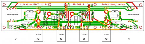
Yes, indeed it does conform to the diyAudio UMS. I do not use Molex connectors for power, gnd, and output. I use #6 thread hex aluminum standoffs instead, primarily because they offer more flexibility in placement.
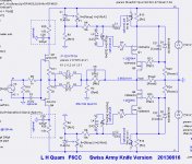
Here is the LTSpice schematic and ExpressPCB artwork. I will rework the schematic to provide component values instead of expressions once I tweak the design on the bench. The PC board layout permits the transformer, input stage, and feedback network to be placed at either end like Nelson does in his F6. I accomplish the same with a single board rather than one designed for each side on the chassis. The cascode MOSFETs are located in the best spot for heat dissipation, assuming a heatsink approximately 10 inches wide. There are a number of optional components, as indicated on the schematic. If the components are not used, jumper wires must be added. I considered the alternative adding traces for those connections which must be cut if the option were to be used. If people like that idea I can do that in the next run of boards.
Attachments
Last edited:
No, I used the ObamaCare inter agency flowchart.Did you use Apple Maps for trace routing?

Great job on the schematic and PCB. Your creations are an example of innovation. I like the inclusion of the resistors [1.5 K] on the drains of the front end. They are an opportunity [for me] to feedforward signal and/or simultaneously bias the output stage.Yes, indeed it does conform to the diyAudio UMS. I do not use Molex connectors for power, gnd, and output. I use #6 thread hex aluminum standoffs instead, primarily because they offer more flexibility in placement.
Here is the LTSpice schematic and ExpressPCB artwork. I will rework the schematic to provide component values instead of expressions once I tweak the design on the bench. The PC board layout permits the transformer, input stage, and feedback network to be placed at either end like Nelson does in his F6. I accomplish the same with a single board rather than one designed for each side on the chassis. The cascode MOSFETs are located in the best spot for heat dissipation, assuming a heatsink approximately 10 inches wide. There are a number of optional components, as indicated on the schematic. If the components are not used, jumper wires must be added. I considered the alternative adding traces for those connections which must be cut if the option were to be used. If people like that idea I can do that in the next run of boards.
Last edited:
Is that cat's name Schrodinger?Is the cat both dean and alive at the same time?
These tested really nice:
An externally hosted image should be here but it was not working when we last tested it.
- Home
- Amplifiers
- Pass Labs
- F6 Amplifier