attached
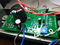
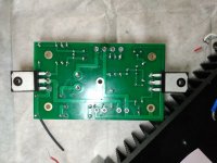
FFT4ME: Your solders look like little balls on most of the resistors. They should look like cones that are wide at the bottom and come to a point at the lead, like they do on Q1. What sort of soldering iron are you using? It looks like you are using too low a heat setting, or you are not keeping the iron on the pad and lead long enough, or a bit of both. You need to reflow the solders so they all look like Q1. When you were working on the other side of the board, it seems that your used too much solder, as there is too much of it on the side pictured. This makes me think that there is a possibility of there being shorts on the other side.
Last edited:
@tizman I'm using a 40w iron I picked up locally. Those balls are what leaked through the hole. I was soldering on the other side and they look like cones there, but the flux I guess let the solder flow through the hole which is what made the balls on the other side.
On the other side the board, the connections look like Q1.
On the other side the board, the connections look like Q1.
........................
In looking at the schematic and based on some of the voltages around Q4, I'm fearing I applied too much heat when soldering and I fried Q4. I'm hoping that's not the case.
......................
I have to agree with you. The voltages around Q4 are not good - way too high at the source side so probably toasted.
The CCS doesn't look good either so really possible that the ZTX450 is a goner too.
It looks like a lot of heat for a long time for the solder to flow through and form a ball at the opposite side .


On the bottom picture ,the red wire on volt + looks like it might not be making a good connection.attached
I have to agree with you. The voltages around Q4 are not good - way too high at the source side so probably toasted.
The CCS doesn't look good either so really possible that the ZTX450 is a goner too.
It looks like a lot of heat for a long time for the solder to flow through and form a ball at the opposite side .
I think you are correct. Too much heat for too long. Years ago, I made lots of poor solder joints until I got a proper iron and improved my technique. Iron may also not be hot enough. Most solders I do these days are done in about 3-4 seconds. My poor solders were done at too low a temperature and for too long. This also causes components to heat up more than a hot iron and a quick solder.
Just to give some different tests: I agree that those blobs look “suspicious”.
When I did mine, I went through the schematic and tested for continuity between the leg of one resistor and the leg of another element that would be “next in line” to be connected. That way I ensured there was a proper solder on leg 1 on one resistor and leg 2 of the other. Also, I did the opposite and measured there was NO continuity between adjacent legs of Jfets, for example.
I’d start there to just confirm all is soldered correctly and making contact as it should.
Just to give some different tests: I agree that those blobs look “suspicious”.
When I did mine, I went through the schematic and tested for continuity between the leg of one resistor and the leg of another element that would be “next in line” to be connected. That way I ensured there was a proper solder on leg 1 on one resistor and leg 2 of the other. Also, I did the opposite and measured there was NO continuity between adjacent legs of Jfets, for example.
I’d start there to just confirm all is soldered correctly and making contact as it should.
This is good advice.
Also, I would get the iron very hot, and quickly reflow the joints on the blob side. It’s got to be quick. Make them melt, and pull your iron away. I suspect that the iron is sub par. That’s my primary concern. Those blobs shouldn’t be there. They should look more flattened or cone shaped like the Q1 solder.
The solder connections to Q1 and Q2 don't look bad from the side of the PCB shown in the pictures. The Voltage readings on Q1 are troublesome however. The maximum Gate to Source Voltage of most IRF fets is 20V. Over Voltage causes the fets to short, Drain to Source. This will show with an Ohmmeter test with the power off, a very low resistance no matter which way (+/-) the meter is connected.
... I gave the boards a once over and I don't see any cold solder joints or solder bridges (even though I was a bit heavy handed with the solder I'll admit). If that's the verdict based on my testing results below then I'll do it again.
Does anyone have any suggestions where to start? If you can take a second to explain why as well that would be great. I'm trying to learn. ...
A solder bridge looks likely as has been mentioned.
Did you see the resistance checks in the trouble shooting guide step 56? Amp Camp Amp V1.6 Build Guide - diyAudio Guides
Let us know what you get please.
Attachments

Thanks to all of you for your help on this. I really appreciate it.
@Kingsportal - I checked the connection and it seems solid, but as others mentioned I may need to reflow the joints.
@Ben Mah and @tizman - As far as soldering time, that's all I used was 3-4 seconds. Could a 40w iron be too much? could the iron be poorly calibrated for temperature and its way hotter than it should be?
@RafaPolit - I'll try that after work today. Thanks!
@Loudthud - Can you define "low"? I hooked up the ohm meter on Q1 between S and D and got 570 ohms both ways. Does this mean Q1 was collaterial damange on this?
@Alan4411 - Thanks for the tip... when I first looked at it I thought maybe I swapped transistors or I had it in backward, but after putting on my reading glasses and using a magnifying glass besides, Q3 has 2 flat faces, and the larger of the 2 flatter faces is aligned with the flat face on the silkscreen.
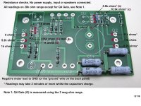
As for the resistor values, I got some clips so that for the measurements that need capacitor charge I could just let it sit and stabilize without me having to hold it. Here are the results:
test pt ; expected ; measured
R15 (b) ; 5.8k ; 4.6k
R15(e) ; 5.2k ; 3.9k
R5(c) ; 10.9k ; 10.2k
Q2(g) ; 11k ; 10.3k
Q2(d) ; 1k ; 0.6 k
Q2(s) ; 5.2k ; 4.1k
Q4(d) ; 1k ; 0.45k
R10(g); 335k ; 0.125M
R9(s) ; 1k ; 0.49k
Q1(s) ; 0 ; 0
Q1(d) ; 5.2k ; 4.1k
Q1(g) ; 1k ; 0.55k
Right now I'm thinking on this board- assuming I do some reflow work and I get similar results, that Q3, Q4 and Q1 need replacement based on feedback. Does this seem right?
@Kingsportal - I checked the connection and it seems solid, but as others mentioned I may need to reflow the joints.
@Ben Mah and @tizman - As far as soldering time, that's all I used was 3-4 seconds. Could a 40w iron be too much? could the iron be poorly calibrated for temperature and its way hotter than it should be?
@RafaPolit - I'll try that after work today. Thanks!
@Loudthud - Can you define "low"? I hooked up the ohm meter on Q1 between S and D and got 570 ohms both ways. Does this mean Q1 was collaterial damange on this?
@Alan4411 - Thanks for the tip... when I first looked at it I thought maybe I swapped transistors or I had it in backward, but after putting on my reading glasses and using a magnifying glass besides, Q3 has 2 flat faces, and the larger of the 2 flatter faces is aligned with the flat face on the silkscreen.
As for the resistor values, I got some clips so that for the measurements that need capacitor charge I could just let it sit and stabilize without me having to hold it. Here are the results:
test pt ; expected ; measured
R15 (b) ; 5.8k ; 4.6k
R15(e) ; 5.2k ; 3.9k
R5(c) ; 10.9k ; 10.2k
Q2(g) ; 11k ; 10.3k
Q2(d) ; 1k ; 0.6 k
Q2(s) ; 5.2k ; 4.1k
Q4(d) ; 1k ; 0.45k
R10(g); 335k ; 0.125M
R9(s) ; 1k ; 0.49k
Q1(s) ; 0 ; 0
Q1(d) ; 5.2k ; 4.1k
Q1(g) ; 1k ; 0.55k
Right now I'm thinking on this board- assuming I do some reflow work and I get similar results, that Q3, Q4 and Q1 need replacement based on feedback. Does this seem right?
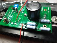
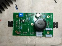
Ok I did some reflow work on the top with some flux and a solder sucker trying to clean things up. I also took the board out of the unit to make it easier to work on. Attaching pics of the cleaned up board (except for flux, I havent removed that yet.
I took measurements again and some surprised me. Here's the current set of measurements with the PCB out of the case:
test pt ; expected ; measured
R15 (b) ; 5.8k ; 4.7k (was 4.6k)
R15(e) ; 5.2k ; 4.0k (was 3.9k)
R5(c) ; 10.9k ; 10.9k (was 10.2k)
Q2(g) ; 11k ; 11.5k (was 10.3k)
Q2(d) ; 1k ; 1k (was 0.6 k)
Q2(s) ; 5.2k ; 3.5k (was 4.1k)
Q4(d) ; 1k ; 1k (was 0.45k)
R10(g); 335k ; 0.20M (was 0.125M)
R9(s) ; 1k ; 1.0k (was 0.49k)
Q1(s) ; 0 ; 0 (no change)
Q1(d) ; 5.2k ; 3.7k (was 4.1k)
Q1(g) ; 1k ; 1k (was 0.55k)
Q3 b,c, and e measures got slightly better based on measurement points and Q4 seems to be better now too (except the source resistance seems low). Q1 and Q2 seem to be a bit better too although the resistance is low on a couple of the pins.
Is it worth plugging it back in and seeing if I can bias it, or are some of these values off enough that something else is a culprit?
Attachments
The odd thing there is the low reading for R10(g). You are basically measuring the resistance of P1 and R10, so should expect at least 332k ohms. A lower reading suggests something in parallel. A shorted or leaky C3 or a leaky Q4...
Measure the resistance across C3 next please. Compare to the other board you have made. After that the suspicion falls back on Q4.
Measure the resistance across C3 next please. Compare to the other board you have made. After that the suspicion falls back on Q4.
- Home
- Amplifiers
- Pass Labs
- Amp Camp Amp - ACA