Biasing EUVL’s F5X
There are likely a number of ways to set the class A bias of the F5X amplifier. The following will describe the one I used. The recommendations here are only intended as a guide and everyone is encouraged to proceed with caution through this process to prevent damage to your as yet untested amplifier. J
Preparation:
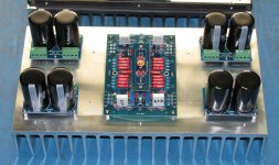
Before starting on biasing you should have your amplifier boards assembled as described earlier in this thread. This includes having the heat sink you intend to use for your amplifier. You should also have two sets of the output quads matched BUT NOT YET INSTALLED.
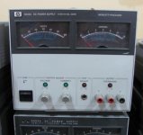
It is also very desirable to have bench top laboratory power supplies with constant voltage (“CV”, adjustable voltage) and constant current (“CC”, adjustable current limit) adjustments. These are what I used so I will describe the procedure with them.
If you do not have laboratory supplies, you can still bias the amplifiers directly with the output from the F5X power supply. You will obviously need to build these first and ensure they are working well with a load of 4 amps per channel. Your dummy load resistor for loading the amplifier output later will work to test the main F5X supplies as long as it can handle at least 200W of power. When the assembly of the F5X supply is complete and it tests OK with no load (a few hundred ohms load minimum is required to test the regulators if used), tie the load resistor from each supply output to ground if you have two 4 ohm loads to use. Do this ONLY WITH THE POWER OFF AND CAPACITORS DRAINED. Alternately, connect the positive supply output through the 8 ohm load resistor directly to the negative supply. Apply power and measure the voltage across each supply to ground. It should be 16V or less +/- 1V. BE CAREFUL as the LOAD RESISTOR(s) WILL GET HOT.
For additional protection if using the F5X supply for bias and testing it is a good idea to add in-line fuse holders from the supply to the amplifier board. You can start out with small fuses when only the front end is tested and work your way up through to the full bias current while changing the fuses to larger ones at each step you increase the bias. The current limit saved my output devices at least once while I was biasing and testing the first board! The fuses might save yours as well…
There are likely a number of ways to set the class A bias of the F5X amplifier. The following will describe the one I used. The recommendations here are only intended as a guide and everyone is encouraged to proceed with caution through this process to prevent damage to your as yet untested amplifier. J
Preparation:
Before starting on biasing you should have your amplifier boards assembled as described earlier in this thread. This includes having the heat sink you intend to use for your amplifier. You should also have two sets of the output quads matched BUT NOT YET INSTALLED.
It is also very desirable to have bench top laboratory power supplies with constant voltage (“CV”, adjustable voltage) and constant current (“CC”, adjustable current limit) adjustments. These are what I used so I will describe the procedure with them.
If you do not have laboratory supplies, you can still bias the amplifiers directly with the output from the F5X power supply. You will obviously need to build these first and ensure they are working well with a load of 4 amps per channel. Your dummy load resistor for loading the amplifier output later will work to test the main F5X supplies as long as it can handle at least 200W of power. When the assembly of the F5X supply is complete and it tests OK with no load (a few hundred ohms load minimum is required to test the regulators if used), tie the load resistor from each supply output to ground if you have two 4 ohm loads to use. Do this ONLY WITH THE POWER OFF AND CAPACITORS DRAINED. Alternately, connect the positive supply output through the 8 ohm load resistor directly to the negative supply. Apply power and measure the voltage across each supply to ground. It should be 16V or less +/- 1V. BE CAREFUL as the LOAD RESISTOR(s) WILL GET HOT.
For additional protection if using the F5X supply for bias and testing it is a good idea to add in-line fuse holders from the supply to the amplifier board. You can start out with small fuses when only the front end is tested and work your way up through to the full bias current while changing the fuses to larger ones at each step you increase the bias. The current limit saved my output devices at least once while I was biasing and testing the first board! The fuses might save yours as well…
Attachments
Setting up:
When wiring up your F5X amplifier boards for first time power up using the bench supplies it is recommended that you include at least some bulk capacitance at the amplifier PCB to minimize potential power supply instability or oscillations. If you are a case subscriber it can simply be the final filter boards for the positive and negative supplies. Make sure to observe correct polarity to and from the filter boards. The “+” marks on the filter PCBs are for capacitor polarity during assembly, not the polarity at the connector!
With the amplifiers disconnected from the power supplies set the supply output voltages to +/-16V. I also recommend you set the current limit (CC setting) to 100mA or less while you test the front end bias. First turn the CC adjustment to the lowest setting. Shorting the output of the power supply will force it into CC mode so that you can set the current limit accurately. CAUTION – if your bench supply does not have a constant current mode shorting the output and powering it up may damage it.
With the power off, wire the bench supply(s) to the amplifier board you wish to test. Make sure to observe the polarity of the positive and negative supply. Any mistakes from this point on could prove catastrophic!
For all of the bias work it is necessary to short the + and – amplifier inputs to ground on the input board.
Measuring the front end bias:
This is done before we install the output devices. We will be measuring the voltage drop across the 11 ohm resistors (the parallel combination of the three resistors that make up R18, R19, R24, or R25) to verify that the front end is working properly and that it is reasonably balanced. Turn on the previously adjusted power supplies to the board. Assuming everything is good there should be no magic smoke and the supplies should not be folding back in CC mode. Measure and note the voltage across resistor R18A, R19A, R24A, and R25A. This voltage divided by 11 is equal to the current flowing through that leg of the front end. This current should fall somewhere within the curve when you matched the J74/K170 sets with the multi-point method described earlier. If everything is working well each measurement will also be very close. If they are grossly different, disconnect power and recheck everything.
This is done before we install the output devices. We will be measuring the voltage drop across the 11 ohm resistors (the parallel combination of the three resistors that make up R18, R19, R24, or R25) to verify that the front end is working properly and that it is reasonably balanced. Turn on the previously adjusted power supplies to the board. Assuming everything is good there should be no magic smoke and the supplies should not be folding back in CC mode. Measure and note the voltage across resistor R18A, R19A, R24A, and R25A. This voltage divided by 11 is equal to the current flowing through that leg of the front end. This current should fall somewhere within the curve when you matched the J74/K170 sets with the multi-point method described earlier. If everything is working well each measurement will also be very close. If they are grossly different, disconnect power and recheck everything.
Attachments
Output bias considerations:
Many push-pull and SE amplifiers have a single bias current adjustment for the output devices. The original F5 amplifier has two - one for each of the complementary output devices. This can make biasing more difficult in that it is necessary to “walk-in” the bias. Setting the top side straight to the target bias and then setting the bottom to the same value will result in not only the first device bias you set being much higher but you will also have large output offsets. Walking-it-in is a method where one of the bias adjustments is brought only part of the way to the final bias value, then doing the same on the other adjustment, again only part way. Checking bias to both devices each time an adjustment is made allows you to gradually approach the final bias value and not overshoot it.
The F5X features four quadrant amplification so it adds to the bias adjustment complexity two additional adjustments per amplifier channel. In order to minimize the hassle (and possible circular pursuit of an elusive bias setting) Patrick included the ability to ground the center point of the amplifier front end. This allows us to treat the F5X as two F5 amplifiers while we bias it. Once we have each side biased and matched relatively well to the other we will change this center connection on the front end and complete the bias in the final X configuration.
Pre-setting the output device gate voltages:
For the initial output device bias setting we want to set it to something lower than full current. If you did a multi-point match of the output devices you should have a list of Vgs voltages necessary to bias the MOSFETs at several different currents. We will use this to preset the gate voltages on the amplifier PCB to get us to the first output stage bias point before ever installing the output devices. You will need to decide which output device will go in each location since even the best matched sets are all slightly different.
Install clip on test leads from the Gate and source pads of one of the output device locations. These are clearly marked in the silkscreen on the PCB. Apply power to the amplifier board and measure the Vgs voltage directly at the FET component pads on the PCB. We want to set this to the gate voltage that the device needs for the lower current of our three point match data. If we assume 1.5A and the necessary gate voltage is 2.0V we will need to adjust the pot for this corner of the amp to this voltage plus the estimated voltage drop across the 0.22R source resistor. Since there is no current flowing through the source resistor right now (no output device installed and therefore no current through) we have to add what this drop will be later on to the initial setting. By doing so the Vgs voltage will be set close to the target value once the output device is installed. The drain resistor will drop this added voltage. Clear as mud, right?
Once all four corners are set in this way it is time to install the output devices. Ensure they are installed in the correct locations, not only for the P and N types, but also for the individual location you assigned to each before we set the initial Vgs pot adjustment above.
For the initial output device bias setting we want to set it to something lower than full current. If you did a multi-point match of the output devices you should have a list of Vgs voltages necessary to bias the MOSFETs at several different currents. We will use this to preset the gate voltages on the amplifier PCB to get us to the first output stage bias point before ever installing the output devices. You will need to decide which output device will go in each location since even the best matched sets are all slightly different.
Install clip on test leads from the Gate and source pads of one of the output device locations. These are clearly marked in the silkscreen on the PCB. Apply power to the amplifier board and measure the Vgs voltage directly at the FET component pads on the PCB. We want to set this to the gate voltage that the device needs for the lower current of our three point match data. If we assume 1.5A and the necessary gate voltage is 2.0V we will need to adjust the pot for this corner of the amp to this voltage plus the estimated voltage drop across the 0.22R source resistor. Since there is no current flowing through the source resistor right now (no output device installed and therefore no current through) we have to add what this drop will be later on to the initial setting. By doing so the Vgs voltage will be set close to the target value once the output device is installed. The drain resistor will drop this added voltage. Clear as mud, right?
If our first device Vgs is 2.0V and we want 1.5A across the FET to start biasing add the drop across the resistor (1.5A * 0.22R = 0.33V) to 2.0V to get the first Vgs target adjustment of 2.33 volts.
Once all four corners are set in this way it is time to install the output devices. Ensure they are installed in the correct locations, not only for the P and N types, but also for the individual location you assigned to each before we set the initial Vgs pot adjustment above.
Powering up for the first time with output devices:
The first time I applied power to each channel I set the bench supply current limit to about 240% greater than the initial bias current I was using, or 2 * 1.5A + 20% = 3.6A. Set this while disconnected from the amplifier.
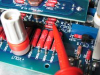
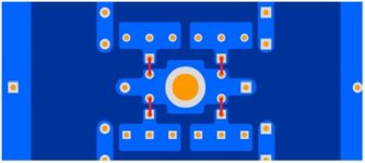
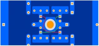
To measure the bias add clip leads to each leg of the 0.22 ohm source resistor for the device you are adjusting as shown below. I also connect a dummy load resistor to the output for the side I am testing. Connect the other end of the load to the local ground at the center of the amplifier PCB.
Apply power and check to see that the bias current is somewhere in the 1.5A range for each device. If the supplies go into current limit something is likely wrong. REMOVE POWER IMMEDIATELY and check for errors. You can measure the current at each source resistor if the lab supply does not include one. The lab supply current meter should read around 3A at this point. Don’t worry if the device bias currents are not exactly equal right now. +/- a few hundred mA is good enough. If everything looks OK at this point leave the assembly on for at least 30 minutes to warm up before adjusting further. Keep checking back to make sure it is still operating at around your initial set point. Once warm it is time to adjust the bias closer to the final value. Don’t forget to increase the current limit on the lab supplies supply the final target of ~4A plus a little margin to keep them out of limit while adjusting.
Adjust one side at a time. Adjust the top and bottom devices on the left (or right) of the PCB to a close balance before moving on to the other. Again, do not go all the way to the final target. Once at the intermediate adjustment point switch over and do the other side. It helps to keep both sides close to the same adjustment for thermal balance and knowing we want them all to be close to equal when operating in balanced mode.
It is important to understand that the bias adjustment setting will not be stable right away. As the heat sink and output devices heat up, the bias current in each device will increase. Often this difference occurs at slightly different rates for even like devices so the adjustment setting for each output device will move more or less than you expect by a small amount as it warms up. For this reason I strongly suggest you adjust in half measures until you get close. What I describe as “half measures” is to walk-it-in by adjusting only halfway or less to where you want it to end up. This way you are less likely to overshoot the final value as everything thermally stabilizes. Taking time between each adjustment is also a good idea. Once close you may find that adjusting in even smaller amounts is the easiest way to get a good bias balance and low offset. Those of you familiar with control systems will appreciate this method. Once you are happy with the bias adjustment of both sides let the amplifier sit powered for around an hour while checking often, and recheck/readjust.
If the bias is very close to equal top-to-bottom and side-to-side on the amplifier it is time to check output offset voltage. Measure the voltage between the output terminal for that side and the center ground terminal. You must have the load connected to do this. Offsets in the few mV to perhaps 50mV are OK right now. Lower is better. If either side is outside of this range re-check the bias of the top and bottom output FET. If these measure very close to the expected value the difference may be because of heat slightly changing the resistance of the source resistors, and therefore the measured current. Simply adjust the top or bottom very slightly to get the bias closer.
The first time I applied power to each channel I set the bench supply current limit to about 240% greater than the initial bias current I was using, or 2 * 1.5A + 20% = 3.6A. Set this while disconnected from the amplifier.
To measure the bias add clip leads to each leg of the 0.22 ohm source resistor for the device you are adjusting as shown below. I also connect a dummy load resistor to the output for the side I am testing. Connect the other end of the load to the local ground at the center of the amplifier PCB.
Apply power and check to see that the bias current is somewhere in the 1.5A range for each device. If the supplies go into current limit something is likely wrong. REMOVE POWER IMMEDIATELY and check for errors. You can measure the current at each source resistor if the lab supply does not include one. The lab supply current meter should read around 3A at this point. Don’t worry if the device bias currents are not exactly equal right now. +/- a few hundred mA is good enough. If everything looks OK at this point leave the assembly on for at least 30 minutes to warm up before adjusting further. Keep checking back to make sure it is still operating at around your initial set point. Once warm it is time to adjust the bias closer to the final value. Don’t forget to increase the current limit on the lab supplies supply the final target of ~4A plus a little margin to keep them out of limit while adjusting.
Adjust one side at a time. Adjust the top and bottom devices on the left (or right) of the PCB to a close balance before moving on to the other. Again, do not go all the way to the final target. Once at the intermediate adjustment point switch over and do the other side. It helps to keep both sides close to the same adjustment for thermal balance and knowing we want them all to be close to equal when operating in balanced mode.
It is important to understand that the bias adjustment setting will not be stable right away. As the heat sink and output devices heat up, the bias current in each device will increase. Often this difference occurs at slightly different rates for even like devices so the adjustment setting for each output device will move more or less than you expect by a small amount as it warms up. For this reason I strongly suggest you adjust in half measures until you get close. What I describe as “half measures” is to walk-it-in by adjusting only halfway or less to where you want it to end up. This way you are less likely to overshoot the final value as everything thermally stabilizes. Taking time between each adjustment is also a good idea. Once close you may find that adjusting in even smaller amounts is the easiest way to get a good bias balance and low offset. Those of you familiar with control systems will appreciate this method. Once you are happy with the bias adjustment of both sides let the amplifier sit powered for around an hour while checking often, and recheck/readjust.
If the bias is very close to equal top-to-bottom and side-to-side on the amplifier it is time to check output offset voltage. Measure the voltage between the output terminal for that side and the center ground terminal. You must have the load connected to do this. Offsets in the few mV to perhaps 50mV are OK right now. Lower is better. If either side is outside of this range re-check the bias of the top and bottom output FET. If these measure very close to the expected value the difference may be because of heat slightly changing the resistance of the source resistors, and therefore the measured current. Simply adjust the top or bottom very slightly to get the bias closer.
Attachments
Amplifier testing:
Once you are happy with the bias for each side you should do some testing before connecting anything to your valuable speakers. You can connect a single ended source to the left side input on the input board referenced to ground. Leave the other side’s input grounded for now. It is desirable to use a 4 ohm load resistor to test each side if available. An 8 ohm load will also work for testing. I use an audio analyzer but it is pretty easy to use a signal generator or sound card and oscilloscope to do some basic testing.
I have used the Dr Jordan Designs software’s free signal generator that will work with most PC system sound cards to make an inexpensive signal generator. I do not have any affiliation with them but I am happy with the product so I mention it here. There may be other signal generators out there as well for free download.
The gain of the amplifier is about 15.6db, a gain of 6. To get 1w out into 4 ohms you will need around 357mV RMS sinewave input. Measure the output of the side under test at the load resistor with an o-scope set on the 2V per division vertical setting. Look for a good clean waveform and check for oscillation. You can do some square wave testing and testing at higher powers if you like as well. Once happy with the first side check the other side of the same amplifier board and both sides of the other channel the same way.
If you are so inclined you can listen to either side individually (essentially an F5 at this point), or connect the input and speaker up in balanced mode and listen to the whole channel in grounded X mode.
Converting to floating X mode:
For initial biasing and testing it was necessary to attach the source of each of the JFETs in the front end to ground. Now that it is up and working it is time to modify it to the floating X configuration. In Floating X configuration, both differential and SE inputs are supported.
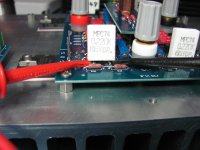
Remove these jumpers original installed on the bottom of the amplifier. You will have to remove the amplifier assembly from the heat sink to do so. It is also helpful for de-soldering and re-soldering here if the amplifier assembly is still warm.
For initial biasing and testing it was necessary to attach the source of each of the JFETs in the front end to ground. Now that it is up and working it is time to modify it to the floating X configuration. In Floating X configuration, both differential and SE inputs are supported.
Remove these jumpers original installed on the bottom of the amplifier. You will have to remove the amplifier assembly from the heat sink to do so. It is also helpful for de-soldering and re-soldering here if the amplifier assembly is still warm.
Attachments
Check bias in floating X mode:
Reconnect both inputs to ground, reassemble the amplifier onto the heat sink, reconnect power, connect a 8 ohm output load resistor from the + output to the - output, and then power the assembly back up. Check the lab supply current meter or measure the voltage drop across each of the 0R22 drain resistors to ensure that the amplifier is operating correctly. Allow the amplifier to come back to temperature while checking the bias current often before moving on.
When converting from grounded X to floating X the bias current at each corner may move a little. Once thermally stable it is necessary to trim these back in. I suggest that you again adjust each corner of the F5X in half measures because you not only will be effecting changes to the other FET bias on that side, you will be changing the output offset. Bring the high ones down a little first and the low ones up a bit. Do this separately on the + and – sides of the amplifier in a back and forth pattern. Do not go too far with any one adjustment without some thermal equalization time in between and checking the others. Take your time here. I adjusted to get the bias balanced as closely as possible and have low offset as measured from the + output to the – output.
Adjust final offset in floating X mode:
As mentioned in the last section, it is helpful to observe output offset as you do the final bias adjustments. Not doing so could lead to a good bias balance on all four corners with several volts of offset. Assuming you have made it to this point with a good bias balance and reasonable offset, tweaking pots at opposite corners should get you the final adjustment.
This final adjustment area is a bit more finesse and art that procedure and instructions can communicate so I invite builders to post questions or experiences that contribute positively to others biasing their F5X successfully.
Test in floating X mode:
If you are like me you will want to test in floating X mode before attaching speakers. Remember that the amplifier is now a floating bridge. The output is from the + to – output pads and not to ground. You can drive the input from a single ended source if you ground the – input but I suggest that you drive the amplifier with a fully balance input to start.
If you are like me you will want to test in floating X mode before attaching speakers. Remember that the amplifier is now a floating bridge. The output is from the + to – output pads and not to ground. You can drive the input from a single ended source if you ground the – input but I suggest that you drive the amplifier with a fully balance input to start.
Last edited:
Well there it is. You should be able to get your amplifier into working condition. Patrick and others will further document the wiring and other case specific details either here or in the case thread. Once the regulator option is flushed out the details will be posted as well.
I still have measurements to make and will be testing output devices that are not close matches from P to N to see how these compare to more closely matched devices. Until then...
Cheers,
Dave
I still have measurements to make and will be testing output devices that are not close matches from P to N to see how these compare to more closely matched devices. Until then...
Cheers,
Dave
I have another volunteer to compare the cascode vs standard.
So that one still to come, but will take a while.
In the meantime, there is enough to keep all those subscribers busy for some time.
Due to requests by PM, I have put up a list for a potential batch 2.
http://www.diyaudio.com/forums/grou...al-euvl-f5x-case-2nd-batch-autumn-2012-a.html
Patrick
So that one still to come, but will take a while.
In the meantime, there is enough to keep all those subscribers busy for some time.
Due to requests by PM, I have put up a list for a potential batch 2.
http://www.diyaudio.com/forums/grou...al-euvl-f5x-case-2nd-batch-autumn-2012-a.html
Patrick
Thank you for this careful explanation Dave.Finding quads in the same range that he uses may be challenging unless you have a large number of parts to select from. In the table below Patrick lists calculated values for the degeneration resistors at various Idss combinations. This is a good place to start with selection based on the datasheets curves for the J74 and K70. Because every transistor is slightly different these numbers will not be exact. Select your parts to configure the front end bias at 5mA or higher (the yellow line and below in chart). A lower value here will dictate changing the drain resistor combination on the amplifier board. You can pre-select your parts with a Rdegen of zero ohms to see what you have, then change the 5 ohm resistor in the matching fixture to the calculated value from the chart. My quads ended up with the best match using 6.8/7.8mA Idss selected parts with 4R degeneration for the J74s.
I think to have understood that if one is in the lucky situation of having sufficient FETs to pick from, one can "simply" do SK170/SJ74 Idss matching with 5R degeneration for the SJ74. Is this correct?
Cheers,
Nic
3 point Idss match? I admit I am a bit confusedYes. But remember the 3 point match.

I can find your test circuit in post#16, but as far as I understand the degeneration resistor is varied here (and not held at a constant 5R).
I guess I will have to study some basic FET function to understand this.......
Thanks,
Nic
Did I say 3 point Idss match ?
3 point match means matching with 3 different degeneration resistors values.
For 2SK170, they are e.g. 0R, 5R, 10R.
For 2SJ74, they are 5R, 10R, 15R.
So the extra 5R degeneration resistor for the 2SJ74 has been taken care of.
As Dave has already explained, one point match is IMHO not sufficiently accurate.
Of course curve tracer match is even better.
Patrick
- Home
- Amplifiers
- Pass Labs
- F5X -- the EUVL Approach - The Build Thread