Hm, I've read it many times but why the gain is 8.5 in practice I don't understand. Perhaps the transconductance plays a greater role here so that a easy fraction won't do the trick.I have played with this a bit and I think you will be fine with Nelsons original values. In practice the gain is about 8.5X so balanced you will get 17X or about 24dB. It also sounds better with Nelsons values. You could also reduce R13 and that will lower the gain also. I haven’t done any listening tests with a lower value R13 but it was fine on the spectrum analyzer.
But as I'm on the hunt for the best music reproduction and as you say the BA-3 sounds best with the original values I'll go this way. Perhaps I'll try to lower R13 to 270 or similar if it seems I need that.
Thank you very much, this was very helpful!
Matthias
Hm, I've read it many times but why the gain is 8.5 in practice I don't understand. Perhaps the transconductance plays a greater role here so that a easy fraction won't do the trick.
...
Thank you very much, this was very helpful!
Matthias
Well, lets go the a basic rough gain fuctions and circuit/application variables calculation. The FE has a pair of JFETs with a transonductance and a RS and an Rdrain. They all play a roll in the basic overall gain. Then there is the Output. The Rs the transconductance and the Rdrain of the output components all play a roll in the overall gain. But, the Rdrain on the Output is mostly dependant on your speaker impeadance

So, if you know all those values then you know the expected Open Loop Gain (OLG). But, the feedback network (Loop) is set up to control gain at the Output. So, the OLG is reduced at the output by the ratio of the feedback resistors as they divert gain back to the input in the form of feedback.
All these values vary somewhat, so I did not use any particular numbers. But, we all do not get the same components, tranconductance in our FET devices, exact resistor/cap values etc. Do we all have 8 ohm speakers?
All of these values are frequency dependant. Therfore the amount of feedback varies with the frequency dependance
not nessarily a good thing!So, "apparent gain" is deffinatly not known until you put "your" speaker on "your" amp. And, as been noted already. Your operating point may sound a little different than someone elses operating point due to all the different componen and speaker tolerances
So, are you sure you want to play with the bias, or any other adjustments or components compared to what Papa has suggested?
Oh yeah, you're right I thought there are no Caps, last time I looked on F4 Schematic is a while ago...
Are there any issues except Noise (Datasheet shows that this is no issue) using 100k in R2, because my Tubepreamp has about 13k Output Impedance?
Thank you and best regards
Felix
I thought there are no Caps, last time I looked on F4 Schematic is a while ago...Are there any issues except Noise (Datasheet shows that this is no issue) using 100k in R2, because my Tubepreamp has about 13k Output Impedance?
Thank you and best regards
Felix
Well naturally some might be confused? But, I just realized I'm comenting on F5 in a BA-3 thread
Actually, I think most everything I said still applies. However the output impeadance of the speaker and the output stage gain actually have very little influence here vs F5. the rest is still valid I believe???
Actually, I think most everything I said still applies. However the output impeadance of the speaker and the output stage gain actually have very little influence here vs F5. the rest is still valid I believe???
Because I ask unnecessary questions I worked a little bit on an AC Analysis of the BA-3
Note for the PushPull BA-2 Output Stage you need C3...
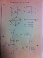
As you can see on the Pictures Voltage Gain mostly depends on transconductance of the 2SK170/2SJ74 and of course R3/R4 and R6/R7 for the first Stage, which is: A1= R6/(R3+(1/Yfs))
Jfets with higher Idss would have higher Voltage Gain!
The Voltage Gain of the Second Stage is: A2= R13/R10+(1/Yfs))
With higher BIAS Voltage Gain can be increased slightly.
Overall Gain is: A= A1*A2*(Rload/(R12+Rload))
I didn't observe fluctuations of Yfs which differs in large Signal conditions!
In this point of view the Bandwidth is infinite
Best regards Felix
Note for the PushPull BA-2 Output Stage you need C3...
As you can see on the Pictures Voltage Gain mostly depends on transconductance of the 2SK170/2SJ74 and of course R3/R4 and R6/R7 for the first Stage, which is: A1= R6/(R3+(1/Yfs))
Jfets with higher Idss would have higher Voltage Gain!
The Voltage Gain of the Second Stage is: A2= R13/R10+(1/Yfs))
With higher BIAS Voltage Gain can be increased slightly.
Overall Gain is: A= A1*A2*(Rload/(R12+Rload))
I didn't observe fluctuations of Yfs which differs in large Signal conditions!
In this point of view the Bandwidth is infinite
Best regards Felix
Attachments
Last edited:
You're right but Papa says this: "The voltage appearing at the Gate of Q3 is amplified by something less than the ratio of R10 divided by R8, and with the same happening at Q4 and considering the transconductance of the Mosfets, comes out at about 15."
and I don't understand it... I think there are more guys who don't understand it
Also Papas explanation is without influences in transconductance
and I don't understand it... I think there are more guys who don't understand it
Also Papas explanation is without influences in transconductance
Because I ask unnecessary questions I worked a little bit on an AC Analysis of the BA-3
Note for the PushPull BA-2 Output Stage you need C3...
As you can see on the Pictures Voltage Gain mostly depends on transconductance of the 2SK170/2SJ74 and of course R3/R4 and R6/R7 for the first Stage, which is: A1= R6/(R3+(1/Yfs))
Jfets with higher Idss would have higher Voltage Gain!
The Voltage Gain of the Second Stage is: A2= R13/R10+(1/Yfs))
With higher BIAS Voltage Gain can be increased slightly.
Overall Gain is: A= A1*A2*(Rload/(R12+Rload))
I didn't observe fluctuations of Yfs which differs in large Signal conditions!
In this point of view the Bandwidth is infinite
Best regards Felix
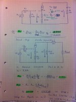
Kamel,
You had it correct and it works out, you just dropped the R5.
So A1=R6/R5+(R3||(P3/2))+(1/Yfs)
First stage 100/100+8.3+45 =.65 gain for first stage and I verified it with my amp.
A2=R13/R10+(1/Yfs)
Second stage 330/22+3.3=13 gain.
For an overall gain of .65*13= 8.45 and that is what we are getting.
Now if you are running balanced you would get 8.45*2 =16.9 or 24.5dB
I’m now satisfied we can calculate the gain correctly.
My copy of the article sez:
The voltage appearing at the Gate of Q3 is amplified by something less than
the ratio of R10 divided by R8, and with the same happening at Q4 and
considering the transconductance of the Mosfets, comes out at about 15.
Both of them added make a system voltage gain of about 30X, or 30 dB.
Obviously it's not clearly written. The voltage gain contributed by Q3 is
about 15 and the voltage gain contributed by Q4 is about 15 and the
result at the output is about 30.
as I wrote in comment #15 of article itself : http://www.diyaudio.com/forums/diyaudio-com-articles/194809-burning-amplifier-ba-3-a.html , there is some discrepancy between text and parts nomenclature ;
Papa , I wrote you about that , also regarding same issue in article on FW site , but it's completely logical that you didn't read that e-mail , considering that I'm sending you approx. 15-25 e-mails/day

anyway - here is , at least by my knowledge , revised text with proper parts nomenclature ( Papa sez , Babelfishing by ZM ) :
Papa , I wrote you about that , also regarding same issue in article on FW site , but it's completely logical that you didn't read that e-mail , considering that I'm sending you approx. 15-25 e-mails/day
anyway - here is , at least by my knowledge , revised text with proper parts nomenclature ( Papa sez , Babelfishing by ZM ) :
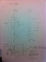
This is familiar enough. Q1 and Q2 are JFETs which self-bias into resistors R3 and R4 at currents around 8 mA. R1 is chosen to avoid oscillatory interaction with whatever source impedance you might have, and R2 provides a DC reference to ground in the event that the source does not, and also establishes the nominal input impedance.
Q1 and Q2 are largely degenerated by R5, setting the amount of AC current which flows through them for a given input voltage. The voltage gain of this initial stage is approximately
the value of Drain load resistors R6 plus R7 divided by R5. In this case we have roughly unity gain – the Jfets are used as unity gain DC level shifters to Q3 and Q4.
Coming off the Drain of Q1 is the loading network of R6, C1 and P2, and there is a comparable network of R7, C2, and P1 attached to the Drain of Q2. R6 clearly sets the AC load for Q1, but the DC requirements to bias up Mosfet Q3 are higher than that, so P2 in parallel with C1 provides a higher resistance value below about 0.5 Hz, and gives the approximately 3 volt DC drop required to bias the Mosfets.
P1 and P2 are adjusted so as to set the DC bias of Q3 and Q4. You will want to set them at zero when you first fire up the circuit, and increase their resistance to achieve the correct bias voltages across R10 and R11 (about 1 volt) while also keeping the output DC offset voltage at a minimum. This circuit is capacitively coupled at the output, but low offset measured at the Drains of Q3 and Q4 will maximize your output voltage swing.
The voltage appearing at the Gate of Q3 is amplified by something less than the ratio of R13 divided by R10, and with the same happening at Q4(R11) and considering the transconductance of the Mosfets, comes out at about 15. Both of them added make a system voltage gain of about 30X, or 30 dB.
R10 and R11 help set the voltage gain, and they also help stabilize the bias of Q3 and Q4, else it would tend to drift upwards as the parts warm up. The bias current here is about 50 mA, and it will deliver peaks of approximately 100 mA. Q3 and Q4 require heat sinks.
Of course you can bias this circuit higher if you wish – 100 mA bias is perfectly OK as long as you properly heat sink Q3 and Q4, and if you are crazy (like me) you can experiment with higher bias, remembering that the parts are rated at 25 watts, and that it costs you voltage losses across R10 and R11. If you want to play with even higher bias, you can consider lowering the values of R10 and R11 and also R13, all in proportion.
The supply voltage is only critical with respect to the voltage rating of the input JFETs, which are nominally 25 volts. In actual testing, they break down around 40 volts. I wouldn't worry about running them as high as 30V. Hot-rodding this circuit would likely involve cascoding the input Jfets to allow higher voltages.
Last edited:
My copy of the article sez:
The voltage appearing at the Gate of Q3 is amplified by something less than
the ratio of R10 divided by R8, and with the same happening at Q4 and
considering the transconductance of the Mosfets, comes out at about 15.
Both of them added make a system voltage gain of about 30X, or 30 dB.
Obviously it's not clearly written. The voltage gain contributed by Q3 is
about 15 and the voltage gain contributed by Q4 is about 15 and the
result at the output is about 30.
I would have thought that Q3 and Q4 being out of phase wouldn’t add together and then the rest of the math works.
My amp has a gain of 8.5X and sounds great. Thank you.
Assumed Gain of first Stage is (R6+R7)/R5 = 2 and of second Stage is (R10+R11)/R13 = 7.5... Overall Gain is 15.
Why adding Gain of upper and lower part of second stage?
When we split it up, so first Stage Gain is R6/R5 = 1 and of second Stage Gain is R13/R10 = 15... overall Gain is still 15?!
The upper half of the Stages only amplify the upper half of the Sine Wave and so second Stage the lower half...
Picture follows...
imagine elastic string between two hands ;
move one hand out and back
move other hand out and back
move both hands out and back
move both hands left and back
move both hands right and back
Oops, you are correct they are in phase, but they still don’t add together, they are push-pull. We are all still getting a gain of 8.5X.
Why adding Gain of upper and lower part of second stage
Neither i get it.
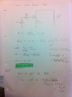
let a 2V pp input signal.
positive half (1v) is amplified 15 times. thats 15v.
Negative half(1v) is amplified 15 times. thats 15v.
output is 30v pp.
That is 15 times 2volts.
Last edited:
.......
Why adding Gain of upper and lower part of second stage?
......
........
........
move both hands out and back
.....
- Home
- Amplifiers
- Pass Labs
- Burning Amp BA-3