Sorry to hear that. Not a ton of parts, and hopefully you have some spares.
Not saying these would be the only things to check before trying to power back up, but here are a few things I'd look at...
Check continuity between all 3 pins of Q4. G to D, G to S, and D to S. All should be OL. If not, Q4 needs replacement.
Measure R8. Should be ~0R5 in circuit. If it shows no resistance or is OL, replace
Replace R14. Should measure ~100R in circuit
Measure R4. Should measure ~10R or less in circuit. If it shows no resistance or is OL, replace
You can sort of check the JFET Q2 - D to S should be <100R or so. G to D and G to S should be 50k ish.
If the gate / source of Q4 failed closed (not sure how MOSFETs typically fail) and Q3 was "off" since you adjusted P1 .... that might explain a bit, with much more than expected current running through R8, Q4, R14, Q2, R4
Do same for similar components on positive rail side.
Note.. if you have a Variac and/or a low (5W candle or something) wattage bulb for your dim bulb tester, you can do the checks, and power up more slowly...
Just as a precaution... I'd keep the other board disconnected while troubleshooting.
As always.. I try to help from the perspective of a relatively new person to all of this also. Nothing I've advised should hurt anything, and you can most likely get to a solution. However, I'm hardly an EE either.
Others likely have some far more concise / better advise, but the usual awesome suspects haven't chimed in yet.
It stinks (sometimes literally) smoking components, but ... it's part of the fun. When you get it working again, you'll be even happier.
Edited to add - measurements only need to be relatively close. I'd only be concerned if something that's supposed to be XXk ohms is closed, open or in the Mohm range or if something that is supposed to only be a few ohms is open or reading 0.
I'm back after receiving the gift of my wife's cold. I have measured the pots as you described and they are low now. They may have been high, but now they aren't, I can't remember back four days. In measuring the pots the bias pot seemed hinky so I replaced it.Hey Chip,
Standard question: Did you verify that P1 and P2 are in the minimal position before power up by measuring the resistance acrosss R5 and R6 and adjusting P1 and P2 so that those resistance measurements are low (near zero or just a few ohms)?
Dennis
I have also corrected the resistor values I had messed up.
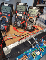
I passed the DBT and PSU measured 47.6 +/-. But when I started to bias, the Bias meters don't move, but the offset does. See photo. When I turn up the bias pot, only the offset increases. The Mosfets don't get warm. I don't think the Jfets were affected.
Still stuck in a puzzle.
Attachments
Chip,
1) Please clarify the quote in IAIMH's post above. Was that just a typo and you meant +/-23.8V (or 47.6V peak-to-peak)?) As always, you need to be precise with your notation.
2) I cannot see exactly how you have the meters hooked up. Do you have one meter measuring the voltage across each of the 0.47R power resistors?
3) Please measure the voltages across R3 and R4. They are the 10 ohm resistors. Use mV scale since their values should be low. That will give an indication of the state of the jfets.
4) How much did you turn the P1 and P2 pots? Assuming the 'bias' meters are measuring voltages across the 0.47R resistors then you seem to be getting some current through one of mosfets (the 0.004V). Not a lot, but something. Recall that depending on the Idss of the jfets you may need a good number of turns before the voltages across R5 and R6 are enough to turn on the mosfets. Perhaps you just need to turn the pots some more?
5) If you still cannot get things to bias correctly, please post a larger, clear, in-focus photo of your PCB. It may help with verifying parts and placement and spotting possible issues.
Dennis,
It appears my cold is still knocking out IQ points around here. Perhaps I should delegate my responsibilities managing the nuclear plant in Springfield to Homer.
1) Yes. I meant 23.8V =/-.
2) Meters were on the 0.47R resistors
3) I have now biased successfully. See photo. Would appear I just didn't turn far enough. I was thrown off by the high offset reading when I began.
R3 and R4 measure 063.3 and -064.2 DCmV
I'll let it simmer for awhile.
Attachments


6L6,Well phooey.
I was obviously looking at the original F5 schematic when I rattled off those resistor positions.
The feedback resistors, the 4 big ones in the middle that connect the amplifier output to the jfets, should be 220ohm.
The output mosfet source resistors, currently you have big green ones, need to be 0.47ohm.
Thanks agian for the help and the original nudge to try out 220R resistors in the R9 - R12 resistors. In your #514 thread you said people reported wonderful sound from the change. I agree. I was just listening to Ricki Lee Jones 1st album, and she was leaping out of the speakers.
Why does an increase of 120 X 4 = 480R change the sound profile so beneficially?

I think, you are speaking about the feedback resistors. I try to explain:
Originally, there are 4 x 100 ohm resistors in parallel = 25 Ohm feedback path
Now, you increased to 4 x 220 ohm wich is resulting in 55 Ohm feedback path
Conclusion: less feedback
Originally, there are 4 x 100 ohm resistors in parallel = 25 Ohm feedback path
Now, you increased to 4 x 220 ohm wich is resulting in 55 Ohm feedback path
Conclusion: less feedback
I would appreciate if anyone could suggest reasons for the following fault for an F5 build?
During establishment of the bias voltage on both channels, I can achieve a balanced 0.4V with no voltage recorded between the poles of the output, all remains stable.
Increasing the bias voltage to the target 0.59V is fine on both channels initially, however after 10 minutes the voltage recorded over R12 (R0.47W) falls dramatically on one of the two channels, the power fuse in the mains switch blows. Upon inspection the ZTX450 has blown, all other components remain OK. This has happened on a number of occasions, always the same fault.
The thermal contact between the npn-mosfet and heat dissipators of the box is good and electrically isolating. The power supply is recording +24 & -24V respectively, no change with time.
All thoughts welcome and appreciated.
Regards
Neil
^ Show some pics, please. Initial thought is thermal runaway. I'd consider looking at the thermistor arrangement first, but w/o pics and more information, it's a tough thing to troubleshoot. Mine is only speculative. Others will likely have other ideas.
I thought I had seen some posts earlier in the thread re: how to continuously monitor voltages as the amp hopefully reaches thermal equilibrium, but I can't seem to find them... maybe that was in the Turbo thread.
I thought I had seen some posts earlier in the thread re: how to continuously monitor voltages as the amp hopefully reaches thermal equilibrium, but I can't seem to find them... maybe that was in the Turbo thread.
![IMG_0527[1].JPG](/community/data/attachments/1079/1079842-d02b2af8b8be9b92c97971b7c90ca92b.jpg)
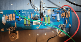
From the pic it looks like thermistor is touching mosfet plastic but I do not see any thermal paste between thermistor and mosfet body, can you please confirm. If yes, try some paste between thermistor and mosfet body.photo attached, the thermistors making direct contact with the MOSFET, the leads of the thermistors are not shorting to any secondary solder joint. I can see why you might have been drawn to thermal management.
Help - F5 Fire and Smoke !!!
I just finished building an F5 amp, V3, using PCBs, JFETs and MOSFETs from the DiyStore… other parts I sourced from Mouser and DigiKey using the V3 BOM and schematic.
I was starting to try and set the bias. I first unplugged both amp boards from the PSU, plugged in the line cord (117 volts AC) measured the rails at the filter boards, got +25 and -25 volts. I set P1 and P2 fully counter-clockwise, so the resistance across R5 and R6 was close to zero. I set P3 to mid-point.
I then connected ONE amp board to the Power Supply (V+, V- and Gnd) then switched on the power - immediately got sparks and smoke, and turned off the power. Upon inspection, the thermistor TH1, on the right side of the PCB, (touching the P channel MOSFET IRFP9141) was charred. I thought maybe it shorted out to the heat sink, or something, so I bent it back so it didn’t touch the MOSFET, and turned on the power again. No smoke from the thermistor, BUT, R8 lit up, becoming incandescent. I immediately shut off the power.
Interestingly the V- supply immediately dropped to zero, but the V+ supply took about 2 minutes before dropping to zero volts.
I checked the orientation of all the JFETs, transistors and MOSFETS, It seems like I have them all in the right positions.
I looked for solder and wire whiskers, cold joints...
I’m not sure where to start looking … I’m not a noob, but I’m not an EE either. I’ve built half a dozen audio projects, all successful, both tubes and solid state devices. Just finished an AmpCamp Amp with no issues.
Any help as to what to check, or a safe method for trying to bring the board up would be appreciated.
Pics and closeups are enclose in case that helps.
thanks
Hello,
I am no expert either, my advise is to take out components and test them. Remove damaged components. Once all components are stuffed in, follow the build guide and use bulb tester for initial biasing.
If something blows up, do not power amp again until issue is fixed, will save lot of components and cost.
How was thermistor mounted, what was it touching?
Last edited:
pretty much everything covered
fact that neg rail is losing juice fast means mosfet on neg side toasted
first thing to be suspicious - were trimpots really zeroed during start-up?
if yes, there was some other mishap - either mosfet short to htsnk or misplaced component(s)
fact that neg rail is losing juice fast means mosfet on neg side toasted
first thing to be suspicious - were trimpots really zeroed during start-up?
if yes, there was some other mishap - either mosfet short to htsnk or misplaced component(s)
- Home
- Amplifiers
- Pass Labs
- An illustrated guide to building an F5