> 2SK3497 is unobtanium, any recommended alternatives?
We have hundreds. Not yet all matched.
See post #1273 and discussions after.
For thermal design, see :
https://linearaudio.net/sites/linearaudio.net/files/v3 euvl.pdf
Patrick
We have hundreds. Not yet all matched.
See post #1273 and discussions after.
For thermal design, see :
https://linearaudio.net/sites/linearaudio.net/files/v3 euvl.pdf
Patrick
FW J2 dissipates 200W of energy not that power at the speakers.
There you have 30W into 8Ohms per channel or 20W into 4 Ohms per channel.
The heatsinks need to dissipate all the 200W but NP likes to run his amps hot, typical 50ºC at the outside of heatsink.
But if you live in a warm climate, as is summer here is Portugal, ambient temp is way over 30ºC normally and many days over 40ºC so these 50ºC become much more than that.
It seems that will not be an issue to you , reference is usually 20ºC ambient temp, for us southern folks a good solution is the "babysitter" that ZM has made popular here ie: a base with fans for the amplifier, these can be run at low voltage just to move the air through the fins, this is very efficient and can be made to look really nice as the base of the amp.
Papa is pretty liberate with numbers , when rails and heat-watts are in case ......which I can explain only with his ( well known ) lazynesssssss
 - I caught him few times in plain and pure copy-paste operations , when writing Manuals
anyway - that's good thing , just few more details enabling Greedy Boyz to use brain ( who's having it , not me Bubba )
J2 is well bellow 100W of heat per side
I believe hottest FW amp - as production piece , not prototype - is SIT-1 - that thing is melting paint from walls and shelves , if you aren't careful
conclusion - make it as you wish , anything from 35W of heat per output device is OK ....... and I'm good for figure of 45W per Semisouth , when cooled well
As an FYI for those looking...
Toshiba 2SJ109 Dual Monolithic Low Noise J-FET | eBay
Are these legit? Has anyone bought and tried these?
We probably still have 10k+ of various unobtanium FETs in stock.
But this is nothing compared to the millions that Nelson has.
He is the Don, not me.
")
And we do intend to release many of those in the next years to keep discrete DIY alive.
Just that it takes a lot of time to match them first.
Patrick
But this is nothing compared to the millions that Nelson has.
He is the Don, not me.
And we do intend to release many of those in the next years to keep discrete DIY alive.
Just that it takes a lot of time to match them first.
Patrick
We probably still have 10k+ of various unobtanium FETs in stock.
But this is nothing compared to the millions that Nelson has.
He is the Don, not me.
He is for sure. Papa always delivers!
And we do intend to release many of those in the next years to keep discrete DIY alive.
Just that it takes a lot of time to match them first.
Being just a hobby for you, this is very noble.
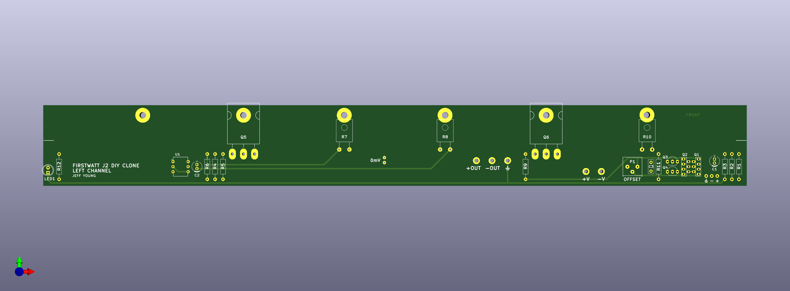
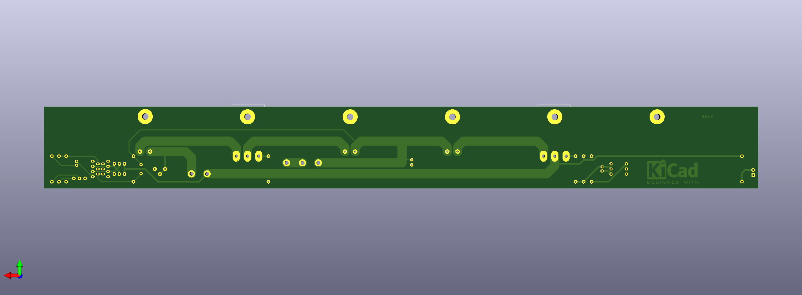
which Is schematic for pcbs
Patrick post 1286 ?
BOM?
Patrick post 1286 ?
BOM?
I'm going to order up a set of these boards for myself. If anyone else is interested, give a shout.
The LTP layout is for a pair of SJ109s (although 4 SJ74s can be inserted in the same holes); the CCS layout is for a pair of SK170s.
Note that they'll be on the expensive side as they're large, I'm getting them done at EuroCircuits rather than a Chinese board house, and volume is likely to be no more than a handful.
Cheers,
Jeff.
which Is schematic for pcbs
Patrick post 1286 ?
BOM?
No, it's an evolution of my design from post 1151 with standard FirstWatt rail voltages and the doubled-up-Panasonics replaced with Ohmites.
Preliminary BOM attached. (The BOM specifies a SemiSouth JFET for the CCS, but you can of course substitute other FETs as detailed in this thread.)
Cheers,
Jeff.
Attachments
Hi Jeff
I just added myself to the GB list. The F3 boards you designed from Euro were very nice, I’m sure these will be too. I know I won’t get to either the F3 or J2 for a while, but I already hoarded the Semisouth and J109 so...
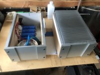
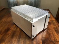
I saw your post of your chassis work pic...here’s one of the mono block chassis’ I’m getting close to finishing for my F2J in progress.
They started as a sort of universal power supply case...then I decided to use heatsinks as a lid.
I have about 8 of the same sink, so any boards I have that are less than 12 inches could be mounted on a sink and swapped out (wish I had made them longer).
The supply will be my first point to point. I’m thinking it could just be re-wired with an additional bridge, thermistors etc once a dual rail supply is needed.
I just added myself to the GB list. The F3 boards you designed from Euro were very nice, I’m sure these will be too. I know I won’t get to either the F3 or J2 for a while, but I already hoarded the Semisouth and J109 so...
I saw your post of your chassis work pic...here’s one of the mono block chassis’ I’m getting close to finishing for my F2J in progress.
They started as a sort of universal power supply case...then I decided to use heatsinks as a lid.
I have about 8 of the same sink, so any boards I have that are less than 12 inches could be mounted on a sink and swapped out (wish I had made them longer).
The supply will be my first point to point. I’m thinking it could just be re-wired with an additional bridge, thermistors etc once a dual rail supply is needed.
Attachments
I wanted to know whether I can adjust the schematics such that it can be optimised to drive a 3R load without parelleling output devices.
Well, you can, by changing a few things, including to 16V rails and 2A bias.
And it would be useful also for 8R loads, even up to 10Vrms output.
Cheers,
Patrick
.
Well, you can, by changing a few things, including to 16V rails and 2A bias.
And it would be useful also for 8R loads, even up to 10Vrms output.
Cheers,
Patrick
.
Attachments
As an FYI for those looking...
Toshiba 2SJ109 Dual Monolithic Low Noise J-FET | eBay
Are these legit? Has anyone bought and tried these?
I bought a pair earlier in the year but a screw up with the test rig I cobbled together fritzed one ..
.. sux I know. I was planning to use them for an Aleph J but the store's board layout doesn't really lend itself to a straight forward fit from this style of component. One for the learning curve on my part.Following that learning experience, I got myself a Peak DCA75. The unit was purchased without a calibration certificate but (according to Peak) all units are calibrated as part of the production QA process.
Refer the attached for the test runs that I logged of the surviving 2SJ109. There are 2 files. The A and B files relate to the respective JFETs in the monolithic component.
From use with the tester, I observed that there was little bit of drift in the results associated with subsequent tests. So, I ended up logging the results of the 5th consecutive test. That seemed to give stable results.
Best efforts to help but please be aware that I'm not a electrickery techo wunderkind.
My read of the results are that the component that I tested is legit. Here are the summary results (sheet marked "ID" from the attachment):
P-Ch JFET
Green-G, Symmetrical Src/Drn
Vgs(off)=-0.49V at Id=4.6µA
Vgs(on)=-0.11V at Id=4.99mA
gfs=29.4mA/V at Id=3.0mA to 5.0mA
Idss=8.78mA at Vds=2.35V
Rds(on)=22.4Ω at Id=5.0mA and Vgs=0.0V
If I've misunderstood the data, I'm sure that those who know more will chip in with their advice.
Hope that helps..
Attachments
Nice case!
I did not see any air inlet at bottom and outlet on top...
Yeah...unfortunate result of “engineering on the fly”.
I planned on perforating the bottom plate along the sides with my mill.
As far as the top, I might try elevating the heat sink with some screw heads slightly to create a small gap that runs the length of the case on both sides.
Otherwise I’ll just have to mill some holes through the heat sink flanking where the board mounts on the bottom side.
Still a bit of finishing work to do too. Trying to get the casework done before cold weather prevents me from doing any work outside.
Yes. Caseworking outside before snow arrives.
Winter is coming.
It must be difficult to mount parts on heatsink while
keeping wire short and placed away magnetic field
of transformer. Maybe turn case upside down
and mount on heatsink with bottom as lid?
I guess convection must be better with flat top mounted
heatsink than side mounted. But will the heat in the heatsink be as distrubuted on heatsink as side mounted? Interesting? Maybe you can measure
heatsink temp either way?
Cheers!
Last edited:
I wanted to know whether I can adjust the schematics such that it can be optimised to drive a 3R load without parelleling output devices...
Thank you Patrick, now I can use the second quad to make a another amp
Rth of
Hi, re-read your paper once more. Thanks for making it public!
Just a single detail: You write that
modern TO247 using Keratherm 86/82 has thermal resistance of
3.5C. I think you referred to 2SK1530 when you wrote this.
This device seems to have a rather large metal pad size.
But Vishay IRFP240, SJEP*R100 and 2SK3498 seems to have
much smaller pad size (I see about 170mm2, 190mm2, 250mm2
looking at specsheet/pictures) and thus I get a rather higher
thermal resistance of 6.5C, 5.7C and 4.5C of Keratherm for these.
Btw: I do totally agree with you conclusion that in the end one needs to measure
actual temperature on heatsink.
Thank you Patrick, now I can use the second quad to make a another amp
Yeh. One with 20V+ rails as the original.
And then you can compare.
Patrick
- Home
- Amplifiers
- Pass Labs
- FirstWatt J2