After having built one of the D1V3 clones and tried various mods, I've been left wondering what a straight D1 clone would actually sound like. I guess there is only one way to answer that question ")
I've made some initial experiments with patching a badly laid out p2p mosfet D1 I/V stage and 78/7915 +/-30V psu onto the D1V3. In some quick and dirty tests 2nd and 3rd harmonics were 6db and 10db lower respectively compared with the D1V3 jfet I/V with a 0dB sine test signal. Noise floor is slightly worse but improved layout of the mosfet I/V, and losing the 2 inch wire connection from dac to i/v should clean things up further. The results of listening test were enough to indicate the mosfet I/V isn't overshadowed by the jfet version.
I'm planning to follow the released schematic of the D1 as far as possible, and will retain the three board configuration. An early attempt at rendering the DAC and I/V area based on a small pic looks promising, but seems to require using a 4 layer board.
A big caveat: My intention is to use the Fujitsu VCXO originally used in the D1.
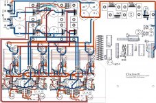
Schematic and parts numbers are as per the d1 service manual schematic.
cheers
Paul
nb: I checked with NP before posting.
I've made some initial experiments with patching a badly laid out p2p mosfet D1 I/V stage and 78/7915 +/-30V psu onto the D1V3. In some quick and dirty tests 2nd and 3rd harmonics were 6db and 10db lower respectively compared with the D1V3 jfet I/V with a 0dB sine test signal. Noise floor is slightly worse but improved layout of the mosfet I/V, and losing the 2 inch wire connection from dac to i/v should clean things up further. The results of listening test were enough to indicate the mosfet I/V isn't overshadowed by the jfet version.
I'm planning to follow the released schematic of the D1 as far as possible, and will retain the three board configuration. An early attempt at rendering the DAC and I/V area based on a small pic looks promising, but seems to require using a 4 layer board.
A big caveat: My intention is to use the Fujitsu VCXO originally used in the D1.
Schematic and parts numbers are as per the d1 service manual schematic.
cheers
Paul
nb: I checked with NP before posting.
a fork in the road
The VCXO is a major issue for this project in that it's scarcity makes the D1 extremely difficult to clone unless you have a Fujitsu VCXO in your possession - no doubt a "good thing" from the Pass Labs perspective.
So at this point I have the choice of pushing on with a clone that is effectively unbuildable except those who already possess the said VCXO, or dumping the D1 VCXO/PLL and replacing it with something based on 2 x Tent Labs VCXO to cover 44.1 and 48/96khz respectively. decisions, decisions....
a potential solution?
One possible "fix" limited to 44.1khz playback would be to add a footprint for a Tent VCXO straddling the fujitsu footprint. This would ignore any frequency switching on the F0 and F1 lines and run at a fixed 44.1khz regardless of input.
A longer term plan if there was any interest would be to make an adapter that plugs into the fujitsu footprint, with relay switching between 11.2896 and 24.576mhz vcxo's. This would enable 44.1khz, 48khz and 96khz playback with a suitable rx and df - cs8414 and df1704 were used in the 24/96 D1.
I'm currently working on the basis of using a cs8414 which has better rejection of data correlated jitter than the cs8412 according to tests posted over at diyhifi.org. The same tests suggest that CS841* have far lower intrinsic jitter than the specs indicate. My current layout is based on the sm5842. This would allow use of a third party adapter to drop in either the sm5847 or df1704.
Paul
spzzzzkt said:The results of listening test were enough to indicate the mosfet I/V isn't overshadowed by the jfet version.
It is good to know that the original mosfet version is holding up well as I might use it to modify a second sacd player. I modified my first one using it and was very satisfied. But I was still wondering whether the jfet version was better. Thanks for the info.
clone mb - some progress
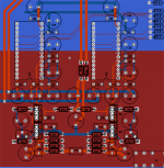
I'm slowly making very slow progress on the D-one clone mother board.
The component placement for the MB is almost final and the routing of the VCXO/PLL and digital power still needs to be done. The attached pic has the ground plane and a top layer polygon shown as outlines only. Cap diameters are sized to allow use of Silmic II's for everything except 1000uf/50V and 3300uf/35V psu caps.
The rx daughterboard is also a work in progress. I've abandoned trying to source the ODL 50 ST module and will use a HFBR-2416 rx and LT1016 comparator as per the datasheet in it's place. There is some discussion on this in the digital forum.
Attachments
Re: clone mb - some progress
Of course, as soon as you post a comment like this you realise that you've got to shuffle half the layout to fix a glaring error. I'd transposed left and right channels, and it only clicked when I worked out how to fix the vast difference in data line length in the layout I posted.
spzzzzkt said:
The component placement for the MB is almost final
Of course, as soon as you post a comment like this you realise that you've got to shuffle half the layout to fix a glaring error. I'd transposed left and right channels, and it only clicked when I worked out how to fix the vast difference in data line length in the layout I posted.
More reworking
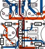
I've been looking at the routing of the 0.01uf caps at the input of the I/V and think I've got that wrong.
I'm not 100% on the purpose of the these caps, but they appear to form a low pass filter with the output impedance of the PCM63. The corner frequency of this filter is just under 24Khz so I suspect it cleans up any RF noise coming from the PCM63.
I'm not sure that the current layout does what is intended??
Attachments
Rip it up and start again....
Thanks to ALDO I have a clearer picture of the layout of the D1 Rev0, and as a result I've ripped up most of the layout I'd done and have reworked the component placement based on this new information.
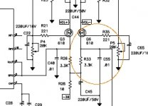
I've noticed that the 3.3K resistors (R26/R33 on the schematic in the post above) in the I/V are different to the rest of the resistors. In the Rev0 dac these appear to be something like holco's while the rest are dale. In the 24/96 version they look like dale RN60's while the other resistors are the standard Pass issue industrial items. It appears the aim is to reduce the noise contribution from this resistor which is at the input of the I/V stage.
At this stage the plan is to do a small run of the boards, which should come in at bit less than $100US for 4 layer motherboard (11.5" x 7.5"), daughter board, and front panel.
Thanks to ALDO I have a clearer picture of the layout of the D1 Rev0, and as a result I've ripped up most of the layout I'd done and have reworked the component placement based on this new information.
I've noticed that the 3.3K resistors (R26/R33 on the schematic in the post above) in the I/V are different to the rest of the resistors. In the Rev0 dac these appear to be something like holco's while the rest are dale. In the 24/96 version they look like dale RN60's while the other resistors are the standard Pass issue industrial items. It appears the aim is to reduce the noise contribution from this resistor which is at the input of the I/V stage.
At this stage the plan is to do a small run of the boards, which should come in at bit less than $100US for 4 layer motherboard (11.5" x 7.5"), daughter board, and front panel.
AT&T RX
I've finally managed to source a handful of AT&T ODL 50 Series II receiver modules. The units are pulls but apparently in very good condition. Anyway this means the daughter board can be done without resorting to a fistful of smd components.
A couple of D1 owning members have very kindly shared pics of the interior which has been extremely helpful.
Current status: I have partial layouts for MB, Daughter board and front panel and have made a start on controller software.
- Status
- This old topic is closed. If you want to reopen this topic, contact a moderator using the "Report Post" button.
- Home
- Amplifiers
- Pass Labs
- D1 clone without enhancements?