Hi Jeff,
I'm a newbie in KiCad... just made my first schematic and PCB.
Have been using MSDOS 6.2 based LAYO1PCB.exe for many years
I'm using 4.07 indeed, in the default mode. Didn't know there were other modes. So the default mode is for me a 25 years progress in PCB design compared to LAYO1
KiCad has a steep learning curve, but I'm getting there...
About the zones, I don't think I am using them? Don't know why I should use them???
I used a zone once, to try to fill the PCB with a copper screen connected to GND. That worked. Looks nice.
Are you filling up this F3 PCB with a copper shield? Papa doesn't do this on his PCB's.
As an old HAM RF amateur I like it very much. Is it because of extra capacitance or crosstalk, that (almost) nobody is using this option?
I 'll continue the hard work on the left channel. I enjoy PCB designing, so it's no big deal. Thanks! Tips are always welcome
Attachments
Check under the View menu and you'll find OpenGL and Cairo. If OpenGL runs, then use it. Otherwise use Cairo.
You'll note that out-of-the-box the traces are no longer transparent. You can fix that by going over to the Layers palette and double-clicking on the little colour boxes.
While zones are most commonly used for things like ground planes, you can also use them to get better control over trace shapes. For instance, if you want to do something like this:

Is that some J2 variant you're working on?
Cheers,
Jeff.
You'll note that out-of-the-box the traces are no longer transparent. You can fix that by going over to the Layers palette and double-clicking on the little colour boxes.
While zones are most commonly used for things like ground planes, you can also use them to get better control over trace shapes. For instance, if you want to do something like this:
Is that some J2 variant you're working on?
Cheers,
Jeff.
Attachments

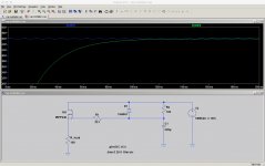
So I'm trying to get my head around the capacitance multiplier in the F3. I think I understand that R19 slows the charging of C5 down so that Q5 turns on slowly, providing a soft-start.
But try as I might I can't get this to simulate in LTSpice. All I get is flat voltage lines. (Well, not actually flat because I'm modelling the residual ripple coming out of my CRC filter so I can see the capacitance multiplier flatten it, but there's no soft-start ramp.)
I've attached my .asc file. Any pointers appreciated.
Cheers,
Jeff.
Attachments
BTW, for anyone else trying to do something like this, the answer is that you need a "UIC" at the end of your .tran statement. (It stands for Use Initial Condition. Otherwise SPICE assumes the circuit has been running since the big bang.)
Screenshot and .asc file attached.
Screenshot and .asc file attached.
Attachments
Regarding Caps for “suds” F3 clone boards
I recently picked a set of unused “suds” F3 clone boards up in the swap meet on impulse.
Since Nelson was nice enough to hand out some more LU1014 recently there had been talk, but not much action on new F3 board group buys.
I suppose it wasn’t entirely on impulse, except I know I already have too much I haven’t built yet.
My excuse is that this is in line with my First Watt amp building exploration.
I already built the ACAs and tweaked them a little with some Semisouth.
My next amp is the F2.
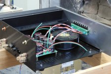
I have already begun assembly of the power supply.
Why not build the PS in a separate case with short umbilicals so it could be used with ACAs, F2 or F3?
Anyway, after doing a bit of research and reading I discovered the source of the GB for these boards and a few under-developed threads related to them.
It seems that a Peter Daniels F3 clone GB was going on at the same time these boards surfaced and there was a BOM posted in the build thread related to these “suds” boards that looks to be more related to the Peter Daniels version and the component kits for them that member jackinnj was offering for sale.
I haven’t worked entirely through this F3 build thread yet. I did get through the discussion about what size capacitor could be used for C1 (which appears to be mislabeled on this “suds” board as C11). I also read through the ideas about using multiple caps in parallel with drivers on the output of the F3.
My issue with these “suds” boards, which I’m hoping someone who may have used them could chime in and help me with, is that in general the spacing of the pads for all the caps appears very small when one considers that the caps specified in these BOMs are rated at 35V and even 63V.
I measured the pad spacing for the caps on these boards center to center with my digital calipers as:
C1(labeled C11) - 10mm
C2,C3,C4,C5,C6,C7 - 3mm
C8 - 3mm
C9 - 5mm
C10 - 3mm
Resistor spacing is 13mm center to center except all the 3watt locations (R3,R4,R5,R6,R7,R8,R9,R10) which were 23mm center to center. None of that looks to present any issues. I still need to find the correct pots for P1,P2 and P3. P3 caught me off guard. Then it occurred to me that it was probably there to adjust for the LED.
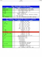
Here is the BOM posted relating to the F3 kits offered by jackinnj:
C1 1 15,000 uF
C10 1 220uF/35V ELNA Silk
C2,C3,C4,C5,C6,C7 6 220uF/63V 493-1356-ND
C8 1 1uF Polypropylene BC2076-ND
C9 1 33pF S.M. 338-1066-ND
D1 1 1N4001 1N4001FSCT-ND
LED1 1 Led BLUE 350-1563-ND
Q1 1 LU1014 Lovoltech Special
Q2,Q3,Q5 1 IRFP240 Matched Triplet IRFP240PBF-ND
Q4 1 ZTX450 NPN Transistor ZTX450-ND
P1,P2 2 5K Bourns Trimpot 3296Y-502LF-ND
R1 1 9.09k 1/4 W 71-CMF55-9.09K-E3
R2,R19 2 47.5K 1/4W 71-CMF5547K500FKEK
R3,R4,R8 3 2R 3W 71-CPF3-F-2
R5 1 2.7R 3W 71-CPF3-J-2.7
R6,R7 2 1R 3W 71-CPF3-F-1
R9 1 0.47R, 3W 283-0.47-RC
R10 1 100R 3W 71-CPF3-100
R11,R21 2 100R 1W 281-100-RC
R12,R22 2 10k 1/4W 71-CMF5510K000FKEK
R13 2 4.75K 1/4W 71-CMF554K7500FHEK
R14,R16,R17,R18 4 1.5K 1/4W 71-CMF551K5000FHEK
R15,R20 2 221R 1/4W 71-CMF55221R00FHEK
I attached a pic of another BOM specifically related to Peter’s GB boards with descriptions of values but without part numbers as well as an image of these “suds” boards.
You can see that the caps specified are either 35V or 63V. I have found nothing in these voltage ratings that will fit the footprints provided on these boards.
So...do I just order the caps specified anyway and bend the leads to fit as best I can and allow the caps to “float” above the boards? Maybe stick a blob of hot glue under them?
All insights/experience are appreciated.
I recently picked a set of unused “suds” F3 clone boards up in the swap meet on impulse.
Since Nelson was nice enough to hand out some more LU1014 recently there had been talk, but not much action on new F3 board group buys.
I suppose it wasn’t entirely on impulse, except I know I already have too much I haven’t built yet.
My excuse is that this is in line with my First Watt amp building exploration.
I already built the ACAs and tweaked them a little with some Semisouth.
My next amp is the F2.
I have already begun assembly of the power supply.
Why not build the PS in a separate case with short umbilicals so it could be used with ACAs, F2 or F3?
Anyway, after doing a bit of research and reading I discovered the source of the GB for these boards and a few under-developed threads related to them.
It seems that a Peter Daniels F3 clone GB was going on at the same time these boards surfaced and there was a BOM posted in the build thread related to these “suds” boards that looks to be more related to the Peter Daniels version and the component kits for them that member jackinnj was offering for sale.
I haven’t worked entirely through this F3 build thread yet. I did get through the discussion about what size capacitor could be used for C1 (which appears to be mislabeled on this “suds” board as C11). I also read through the ideas about using multiple caps in parallel with drivers on the output of the F3.
My issue with these “suds” boards, which I’m hoping someone who may have used them could chime in and help me with, is that in general the spacing of the pads for all the caps appears very small when one considers that the caps specified in these BOMs are rated at 35V and even 63V.
I measured the pad spacing for the caps on these boards center to center with my digital calipers as:
C1(labeled C11) - 10mm
C2,C3,C4,C5,C6,C7 - 3mm
C8 - 3mm
C9 - 5mm
C10 - 3mm
Resistor spacing is 13mm center to center except all the 3watt locations (R3,R4,R5,R6,R7,R8,R9,R10) which were 23mm center to center. None of that looks to present any issues. I still need to find the correct pots for P1,P2 and P3. P3 caught me off guard. Then it occurred to me that it was probably there to adjust for the LED.
Here is the BOM posted relating to the F3 kits offered by jackinnj:
C1 1 15,000 uF
C10 1 220uF/35V ELNA Silk
C2,C3,C4,C5,C6,C7 6 220uF/63V 493-1356-ND
C8 1 1uF Polypropylene BC2076-ND
C9 1 33pF S.M. 338-1066-ND
D1 1 1N4001 1N4001FSCT-ND
LED1 1 Led BLUE 350-1563-ND
Q1 1 LU1014 Lovoltech Special
Q2,Q3,Q5 1 IRFP240 Matched Triplet IRFP240PBF-ND
Q4 1 ZTX450 NPN Transistor ZTX450-ND
P1,P2 2 5K Bourns Trimpot 3296Y-502LF-ND
R1 1 9.09k 1/4 W 71-CMF55-9.09K-E3
R2,R19 2 47.5K 1/4W 71-CMF5547K500FKEK
R3,R4,R8 3 2R 3W 71-CPF3-F-2
R5 1 2.7R 3W 71-CPF3-J-2.7
R6,R7 2 1R 3W 71-CPF3-F-1
R9 1 0.47R, 3W 283-0.47-RC
R10 1 100R 3W 71-CPF3-100
R11,R21 2 100R 1W 281-100-RC
R12,R22 2 10k 1/4W 71-CMF5510K000FKEK
R13 2 4.75K 1/4W 71-CMF554K7500FHEK
R14,R16,R17,R18 4 1.5K 1/4W 71-CMF551K5000FHEK
R15,R20 2 221R 1/4W 71-CMF55221R00FHEK
I attached a pic of another BOM specifically related to Peter’s GB boards with descriptions of values but without part numbers as well as an image of these “suds” boards.
You can see that the caps specified are either 35V or 63V. I have found nothing in these voltage ratings that will fit the footprints provided on these boards.
So...do I just order the caps specified anyway and bend the leads to fit as best I can and allow the caps to “float” above the boards? Maybe stick a blob of hot glue under them?
All insights/experience are appreciated.
Attachments
Those boards look to be problematic. Even aside from the cap spacing issue, the LU1014's have Nelson's upside-down placement, but without the hole in the board to allow them to be mounted on the underside of the heatsink flange. It appears there's a big square pad on the bottom -- did the board designer intend their tabs to be soldered to the back of the board?
My SPICE sim says the Lovoltech is running at about 5W. Soldering to the back of the board seems unlikely to support that kind of dissipation.
Are you in a hurry? You're welcome to my board designs once I test them to make sure they work. While it's somewhat expensive to make single boards, there ought to be others around with Nelson's prezzies that might be interested in a group buy....
Yes, I agree the problems appear to go further than just the footprints provided for the caps.
After checking the LU1014 data sheet for its pinout and then comparing it to the F3 circuit and the board it does appear as if the designer intended the transistor to be mounted on the bottom of the board.
The solder pad looks to be for mounting the body of the LU1014, what good this would do for heat dissipation is beyond me.
I researched the subject of heat sinking the LU1014 in other threads and several people have been very creative in attaching copper “spreaders” to them that in turn mount to their main heatsinks. I’m assuming I would have to do something similar with these boards.
I’m in no hurry. As I said, I have plenty of other projects in que. Getting my hands on these boards naturally raised questions as to how I was going to populate them. I was trying to put together a Mouser order for some other things I needed and wanted to add the F3 components.
I appreciate the offer of making your boards available. I will be keeping an eye on this thread and watching your progress.
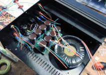
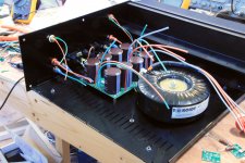
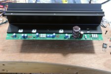
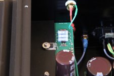
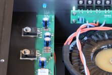
I'm mounting my Lovoltechs on top of the heat-sink flange. Out-of-the-box their legs aren't long enough for this, so they were shortened to just that needed for the horizontal bit, and then resistor leads were added for the vertical bit.
There's a brass bar behind the screw which is the same height as the JFET. It's stuck down with a bit of superglue to make assembly easier.
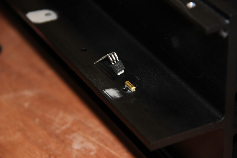
Then the JFET goes down with a bit of grease and mica and a cap screw with a conical washer and then a fender washer.
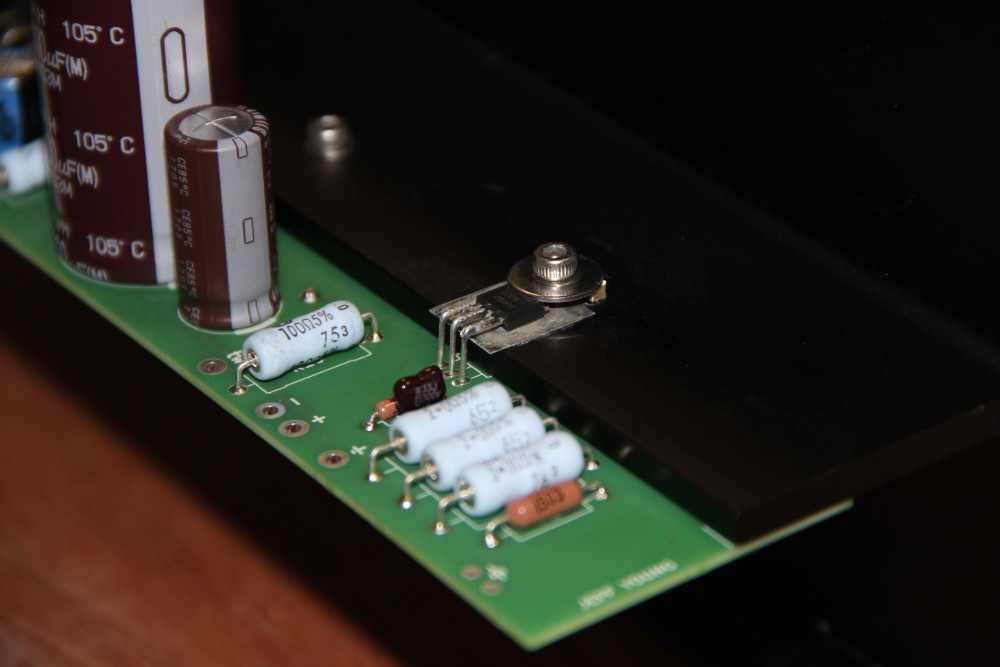
The MOSFETS mounted in conventional fashion:

While running it in it my benchtop PS claimed it was consuming 1.61A.
Temps measured with IR thermometer:
c-multiplier MOSFET case: 48ºC
CCS MOSFET case: 76º
heatsink nearby: 65º
cascode MOSFET case: 72º
JFET case: 44º
heatsink nearby: 40º
outside of heatsink at centre: 44ºC
Offset was at 21V so CCS should be burning 30W for a die temp of 101º.
All seems good enough to build the other channel?
There's a brass bar behind the screw which is the same height as the JFET. It's stuck down with a bit of superglue to make assembly easier.
Then the JFET goes down with a bit of grease and mica and a cap screw with a conical washer and then a fender washer.
The MOSFETS mounted in conventional fashion:
While running it in it my benchtop PS claimed it was consuming 1.61A.
Temps measured with IR thermometer:
c-multiplier MOSFET case: 48ºC
CCS MOSFET case: 76º
heatsink nearby: 65º
cascode MOSFET case: 72º
JFET case: 44º
heatsink nearby: 40º
outside of heatsink at centre: 44ºC
Offset was at 21V so CCS should be burning 30W for a die temp of 101º.
All seems good enough to build the other channel?
Attachments

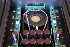
My left channel plays beautiful music, so I've started assembling the right.
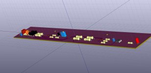
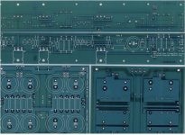
This is the schematic my boards use:

It's identical to the NP design except for the 3 changes mentioned in blue text at the bottom. (I also redrew the c-multiplier so my little brain could better understand it, but it's unchanged.)
I've attached the Kicad project (the .zip file) in case anyone wants to make some. The PCBs contain one additional change beyond the schematic changes: C8 is mounted below board and can accommodate something like a Mundorf Supreme.
Note that the PCBs assume a mounting flange with 2" spaced holes (ie: FirstWatt-style enclosures, not those in the DIYAudio store).


Many board houses accept the *.kicad_pcb files directly. However, if someone wants to make these boards with a board house that doesn't, PM me and I'll generate Gerbers and post them.
I got my boards done at EuroCircuits. When you order low numbers from them you often get extras, so I have two extras of the Left channel. Sadly, no extras of the Right. But if someone wants to order just a Right I'll send you the Lefts for the cost of postage.
Note that while the Kicad project contains a PSU board you can use any standard Pass-suitable PSU board that supports single-rail supplies. I just like to do my own.
Cheers,
Jeff.
This is the schematic my boards use:
It's identical to the NP design except for the 3 changes mentioned in blue text at the bottom. (I also redrew the c-multiplier so my little brain could better understand it, but it's unchanged.)
I've attached the Kicad project (the .zip file) in case anyone wants to make some. The PCBs contain one additional change beyond the schematic changes: C8 is mounted below board and can accommodate something like a Mundorf Supreme.
Note that the PCBs assume a mounting flange with 2" spaced holes (ie: FirstWatt-style enclosures, not those in the DIYAudio store).
Many board houses accept the *.kicad_pcb files directly. However, if someone wants to make these boards with a board house that doesn't, PM me and I'll generate Gerbers and post them.
I got my boards done at EuroCircuits. When you order low numbers from them you often get extras, so I have two extras of the Left channel. Sadly, no extras of the Right. But if someone wants to order just a Right I'll send you the Lefts for the cost of postage.
Note that while the Kicad project contains a PSU board you can use any standard Pass-suitable PSU board that supports single-rail supplies. I just like to do my own.
Cheers,
Jeff.
Attachments
Right channel has been run-in on the bench supply.
Here's an interesting thing: when adjusting the offset POT the voltage takes some time to reflect the change. The temp of the MOSFET cases, though, adjusts much more quickly: I suspect if you just balanced the case temps of the CCS and cascode you'd be pretty near 21V.
Cheers,
Jeff.
Here's an interesting thing: when adjusting the offset POT the voltage takes some time to reflect the change. The temp of the MOSFET cases, though, adjusts much more quickly: I suspect if you just balanced the case temps of the CCS and cascode you'd be pretty near 21V.
Cheers,
Jeff.
Beautiful. Enjoy it in good health.
I had hoped to be working on my new amp. With the holiday demands and my pop in the hospital I just haven’t found any time.
I had thought of extending the legs on the jfets to get them to work on the boards I had as well... but there’s still the issue of the very small footprints for the caps.
If no one has spoken up for the extra boards I would be interested as they look better than the ones I ended up with.
I wonder if I could get Osh Park to make a complete left/right and PS board? I’ve never uploaded or shared a pcb design with them, only ordered boards others have uploaded and shared.
OSH Park will take the *.kicad_pcb files directly, so it should be easy-peasy. (All 3 of them are in the .zip I posted.)
Send me your address by PM if you want the Left boards; no one has spoken for them yet.
(While the BOM is pretty standard, I've attached a list of what I used. Remove the .txt extension and it will open in Excel or Numbers. I'm not sure I'm a believer in boutique caps, but I used Mundorf Supremes for C8 just to be sure. Note that the leads barely fit through the holes, so some wiggling is required.)
Attachments
I managed to install a zip extraction app on my phone and got your files into it.
I went to Osh Park and they had some kind of automated file upload prompt I tried.
It didn’t seem like it would be able to grab the files because I couldn’t export or save them to files with the zip app... then somehow I accidentally got the left channel to upload. Once it had the file and displayed the board with dimensions it quoted a minimum order of 3 copies for about $125. I suppose the right channel would be the same.
Just wondering if that is in line with what you paid? It would probably be better to get the right channels made at the same house if so.
Wow, mine were dear, but not that dear.
Go to: Eurocircuits :: Sign In, upload just the F3 Right.kicad_pcb file and see what they say.
To get the same boards as the Left you'll need to bump up the "Outer layer copper foil" to "35um (end +/- 60um)" and the "Surface finish" to "HAL leadfree".
Order just one and you may get two, and then you'll have another pair to pass on.
- Home
- Amplifiers
- Pass Labs
- F3 Builders Thread