there is a difference between the N and P types.
not so easy to fab.
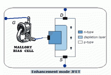
There is no such thing as an enhancement mode JFET. There is no way to create a built in field to adjust the threshold like a MOSFET.
EDIT - It must be happy hour.
Last edited:
There is no such thing as an enhancement mode JFET. There is no way to create a built in field to adjust the threshold like a MOSFET.
of course not.
because you said so.
There is no such thing as an enhancement mode JFET. There is no way to create a built in field to adjust the threshold like a MOSFET.
EDIT - It must be happy hour.
YouTube
of course not.
because you said so.
Sorry physics says so.
...........the process yields what looks like 'blobs' on die,............
There is no such thing as an enhancement mode JFET. There is no way to create a built in field to adjust the threshold like a MOSFET.
EDIT - It must be happy hour.
"Blob" may imply they are hiding something. A teeny battery?
It seems to be happy WEEK. Cheers!
Attachments
How would you call a Semelab SML100M12MSF then?
SML100M12MSF Semelab / TT Electronics | Mouser Europe
SML100M12MSF Semelab / TT Electronics | Mouser Europe
Sorry physics says so.
True for the standard JFET device.
Not true for non standard and a hardly integrable layout and process:
US7180105B2 - Normally off JFET
- Google Patents
How would you call a Semelab SML100M12MSF then?
SML100M12MSF Semelab / TT Electronics | Mouser Europe
Much easier to do on wide bandgap materials like SiC, since they allow forward biasing the JFET gate without much leakage. A heroic effort is required for a normally off silicon JFET, see the above Infineon patent. The “pinch” voltage in this case is limited to some 0.2-0.4V before the exponential gate current kicks in and makes a mess of the conduction mechanism. Under the circumstances, I would think a high channel conductance would require a huge silicon area.
Last edited:
"Blob" may imply they are hiding something. A teeny battery?
It seems to be happy WEEK. Cheers!
Regards
thanks for the advice on transistors way back
Sorry physics says so.
what is this physics you speak of??
here's the small signal
Attachments
Sorry physics says so.
what is this physics you speak of??
revisited
Attachments

- Status
- This old topic is closed. If you want to reopen this topic, contact a moderator using the "Report Post" button.
- Home
- Design & Build
- Parts
- Enhancement mode JFET