Hi everyone...
This seemingly simple job has become a total time vacuum and I'm not really
sure what's going on.
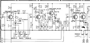
Symptoms: Low output from the preamp & Treble control doesn't work.
Attempted remedies: Rebuild PSU. New e-caps throughout and subbed in for tantalums in the tone section.
Work-arounds: After FET 3 is an effects loop. If I plug my test signal into the return jack, the circuit is very loud and clear. Also, if I plug my test signal directly into the wiper of the treble control, the pot IS responsive.
I'm usually good at spotting previous repair work but this isn't so clear. However, the original parts list shows all FETs in this circuit (9 total) to be SK30A-Y. However, all but FET 1 are actually p/n 2N3819.
I've been pouring over data sheets but I really don't know what I'm doing. Furthermore, I don't generally use NTE subs but the 2 aforementioned FETs call up different NTE part numbers, which makes me suspicious.
Replacing the original SK30A-Y in position 1 with 2N3819 makes the signal way lower... so maybe the original FETs are required to get this going again? But the treble control doesn't work with either...
Can someone please check me on this? I'm certain I'm missing something when it comes to these transistor part numbers.
Thanks!
This seemingly simple job has become a total time vacuum and I'm not really
sure what's going on.
Symptoms: Low output from the preamp & Treble control doesn't work.
Attempted remedies: Rebuild PSU. New e-caps throughout and subbed in for tantalums in the tone section.
Work-arounds: After FET 3 is an effects loop. If I plug my test signal into the return jack, the circuit is very loud and clear. Also, if I plug my test signal directly into the wiper of the treble control, the pot IS responsive.
I'm usually good at spotting previous repair work but this isn't so clear. However, the original parts list shows all FETs in this circuit (9 total) to be SK30A-Y. However, all but FET 1 are actually p/n 2N3819.
I've been pouring over data sheets but I really don't know what I'm doing. Furthermore, I don't generally use NTE subs but the 2 aforementioned FETs call up different NTE part numbers, which makes me suspicious.
Replacing the original SK30A-Y in position 1 with 2N3819 makes the signal way lower... so maybe the original FETs are required to get this going again? But the treble control doesn't work with either...
Can someone please check me on this? I'm certain I'm missing something when it comes to these transistor part numbers.
Thanks!
Attachments
2SK30A and 2N3819 are both N-channel JFETs and SHOULD (always check) have the same pin connections. They ought to be able to work in the same applications.I'd expect Yamaha had to change suppliers in mid-production. The 2SK30A is a 50v part, while the 2N3819 is a 25v part. But unless this preamp is running at over 25v, this will not be an issue. I suspect that explains the NTE situation.
Isolate the problem. Apply a signal to the input, trace with a scope or signal tracer through the circuit. I don't know what the power supply voltage is across the top, 12v maybe? Is that reaching R104, R110? And do FET 1,2 have similar voltages on their drains?
Apply signal and is it amplified to R104? And can you follow that signal through C102, R107, and the rest of the tone stack?
You do know if all the tone controls are at zero, you get no sound?
Thank's for jumping on board!
The supply rail is 12V.
The best I can do for FET 1 is with the original 2SK30AY. All it can muster is 100mV in, 4.5v on the drain, 0.7v on the source. It spits out about 50mV to R104 and the tone stack.
I'm finding conflicting data sheets. I bought the 2N3819 from mouser and their data sheet shows the pin configuration as D - G - S. However, all the OEM 3819's would be backwards if this is correct (D/S reversed)!
Now, for the record, I can't get new or old 2N3819 to do anything in FET1 position. They kill my test signal. About 1.2V on the drain, 1.0V on the source, regardless of OEM/new part or orientation.
Just to check myself on this, I did install FET 2 and 3 with the orientation as dictated by the data sheet - that is, reverse them as I found them originally.
FET 2:
D - 2.6
G - 1.1
S - 2.4
FET 3:
D - 11.7
G - 6.3
S - 8.3
Output signal is decent if my test is injected into FET 3.
Last edited:
D and S can usually be swapped. Depends on teh part and situation.
I NEVER trust the pinouts on data sheets. I ALWAYS check. The JFET by its nature is ON until we turn it off with a gate voltage. SO sitting there alone, you will find with an ohm meter that two legs - the S and D - have a low resistance between them, and the third leg is the gate.
I NEVER trust the pinouts on data sheets. I ALWAYS check. The JFET by its nature is ON until we turn it off with a gate voltage. SO sitting there alone, you will find with an ohm meter that two legs - the S and D - have a low resistance between them, and the third leg is the gate.
More than a few JFETs (but not all of them) are in fact symmetrical in construction, that's why.D and S can usually be swapped. Depends on teh part and situation.
BTW - if "low output and treble control doesn't work", have you (OP) checked the treble pot at all? Might be open or something.
Hmm. Is ~212 nA of gate current an acceptable spec for leakage on the 2SK30A-Y? Seems a tad high for a FET.The best I can do for FET 1 is with the original 2SK30AY. All it can muster is 100mV in, 4.5v on the drain, 0.7v on the source. It spits out about 50mV to R104 and the tone stack.
0.7 V on 1k would be 0.7 mA, or certainly well below the 1.2-3 mA Idss rating of the -Y grade, much like you'd expect. I'd say that aside from some leakage (and potentially increased noise), the FET appears to be working OK. 2N3819 Idss is 2..20 mA, and if you got one on the higher side it is not likely to work very well. 2N5460 might be more like it.
The surface mount (SOT-23) equivalent of 2SK30A apparently is 2SK208, and seemingly 2SK879 as well. Mouser alone has thousands in stock.
Last edited:
As far as I know, if a JFET really knows its D from its S, the difference is a couple pFd of capacitance. In RF work you put the lower-C leg as the "Drain" for slightly increased gain/stability.
In audio builds we do not need/want MHz response and usually we have much more than a few pFd of stray capacitance everywhere, so it makes NO difference.
Can anybody cite a truly asymmetric JFET?
In audio builds we do not need/want MHz response and usually we have much more than a few pFd of stray capacitance everywhere, so it makes NO difference.
Can anybody cite a truly asymmetric JFET?
What is confusing to me is that the entire circuit is running on 2n3819... Why is it causing issues in the first two gain stages. Seems to me FET 3 and onwards are working OK.
Here is the full manual, with schematic across pages 14/15.
What do you guys think.... there are suppliers of the 2SK30AY...not cheap, but at this point it is becoming a headache.
Again, here is where I'm at. With the SK30AY back in the FET 1 position, with all the EQ positions at maximum, I have about 50% signal loss between the Gate and Drain of FET 1. I can see the signal throughout the tone stack and it is making to the gate of FET 2. But, still, FET 2 is producing virtually no signal.
Right now I'm most concerned about why there is 50% signal loss through the first gain stage and why FET 2 doesn't seem to be working.
The answer is in one of your previous posts, where you reported the following DC voltages:...concerned about...why FET 2 doesn't seem to be working.
FET2's drain is 0.2 volts more positive than it's source, meaning that FET is saturated, turned fully on, and therefore unable to amplify.FET 2:
D - 2.6
G - 1.1
S - 2.4
What's happened is that this particular FET has either a larger pinch-off voltage (Vgs_off), or a larger Idss, than the original. So it's trying to flow more current than it can in this particular circuit.
The simple fix is to increase the source resistor, until the drain settles at a reasonable voltage, roughly halfway between the source voltage and supply voltage. If the source ends up at, say, 2.5 volts, and your supply voltage is 12 volts, fiddle with the value of the source resistor until the drain settles somewhere around 7.5 volts, plus or minus a volt or so.
That may not be the original factory value, but at least you know the JFET will work as a linear amplifier when it's centre-biased like that.
JFETs have very wide manufacturing tolerances, and in my experience, can rarely be swapped without having to tweak biasing components to compensate.
P.S. From the schematic, I would estimate FET1 should have a voltage gain of around 5 (somewhere between 5 and 10). It's gate should be at zero volts, so your DMM shouldn't show more than a few millivolts DC there. Make sure the gate coupling cap (C101) isn't leaky, and the FET itself is good.
-Gnobuddy
Last edited:
> Here is the full manual...
Thank You Thank You Thank You !
I worked with that machine around 1980. Good piano and great preamp. Adapted its circuit to a guitar amp which played well. But I had not seen that plan in decades, until you posted it.
> Seems to me FET 3 and onwards are working OK.
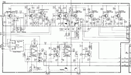
3, 5, 6, 7, 9, 8 are source-followers with a bias which will work on almost any JFET (Vgsoff <4V).
1, 2, 4 are gain-stages and bias is critical. Too far off and you get what you have: "bottomed", drain can't swing except to pass part of a loud signal.
Yamaha could pick ample quantities of JFETs which would bias well with these resistors; they apparently sourced K30s which are a hot little amplifier.
2N3819 is a much older type with higher (actually very wide) bias requirement. However it may be contemporaneous with the CP-70B? Even so, Yama may have been sorting-out crates of '3819 to cherry-pick the low-V ones. Which still does not explain why it does not work today. If you say Yama docs spec 2SK30 and you find 3819, my least-silly guess is that someone plugged a 100W amp to this preamp, blew-up FET1, someone replaced with "any available FET", no luck, and replaced them all before giving up.
Focus on 1, 2, 4. Get them biased like Gnobuddy says. This may be change of source resistor (which will change gain), or finding a 2SK30A-Y-like device which biases good with original values.
Thank You Thank You Thank You !
I worked with that machine around 1980. Good piano and great preamp. Adapted its circuit to a guitar amp which played well. But I had not seen that plan in decades, until you posted it.
> Seems to me FET 3 and onwards are working OK.
3, 5, 6, 7, 9, 8 are source-followers with a bias which will work on almost any JFET (Vgsoff <4V).
1, 2, 4 are gain-stages and bias is critical. Too far off and you get what you have: "bottomed", drain can't swing except to pass part of a loud signal.
Yamaha could pick ample quantities of JFETs which would bias well with these resistors; they apparently sourced K30s which are a hot little amplifier.
2N3819 is a much older type with higher (actually very wide) bias requirement. However it may be contemporaneous with the CP-70B? Even so, Yama may have been sorting-out crates of '3819 to cherry-pick the low-V ones. Which still does not explain why it does not work today. If you say Yama docs spec 2SK30 and you find 3819, my least-silly guess is that someone plugged a 100W amp to this preamp, blew-up FET1, someone replaced with "any available FET", no luck, and replaced them all before giving up.
Focus on 1, 2, 4. Get them biased like Gnobuddy says. This may be change of source resistor (which will change gain), or finding a 2SK30A-Y-like device which biases good with original values.
Attachments
FET2 has its source resistor bypassed with a cap, so changing its source resistor will have a relatively minor and insignificant effect on gain....change of source resistor (which will change gain)...
FET1 & FET4 will indeed change gain with different Rs, but that's probably better than the alternative (the circuit doesn't work.)
In principle you can change Rs till the FET (FET1 or FET4) biases properly, then bypass Rs with a series R-C combination chosen to restore the original gain; pick the second resistor so the parallel combination is 1k as before.
As an example, suppose you had to raise Rs from 1k to 2.2k to get the FET to bias properly; now string a 1.8k resistor in series with a suitable cap (10 uF, say), and wire that combination across the new 2.2k source resistor.
To AC, the cap is a short, so the effective AC source resistance is 2.2k in parallel with 1.8k, which works out to 0.99k, essentially the original value of 1k, which more-or-less preserves the original gain. To DC, the new source resistance is 2.2k, which biases the FET properly. Win-win.
The catch is finding room for the extra RC on what's probably an already crowded PCB. It may not be practical.
There is a similar story told about an old Wampler guitar pedal called the Plexi-Drive, which uses three JFETs.Yamaha could pick ample quantities of JFETs which would bias well with these resistors
Someone opened one up, traced the circuit, and posted it to the internet. Shortly after that one began to read tragic stories about futile attempts to build the circuit, all of which failed to work because not a single JFET could be found that would bias up properly.
Some people went so far as to buy a bag of 50 or a 100 JFETs and sort through the whole lot trying to find three that would work in this circuit. No dice.
Someone inferred from all this that Wampler was using oddball, out-of-spec JFETs hand-selected to work in this particular circuit. Of course crazy tales about magic mojo only available with these unobtanium out-of-spec JFETS immediately followed.
Brian Wampler himself appeared on one of the forums, helpfully commenting that the FETs absolutely had to bias up to 4.5 V at the drain for the circuit to work properly.
I happen to have a few of the same JFETs used in that pedal. I stuck one into a breadboard with the drain resistor shown in the ripped-off Plexi-Drive schematic, and tweaked the source resistor until the JFET biased properly. It took 3.3k, where the (ripped-off) schematic had shown 1k.
Curious, I tried more JFETs from my stash. Every single one I tried biased up perfectly with Rs = 3.3k. Every single one was saturated, full-on, with Rs = 1k.
My guess is that the person who traced the original circuit mis-read the colour codes on the source resistor. It never was 1k. Wampler is a small boutique manufacturer, not a giant like Yamaha. IMO there's very little chance that Wampler was sorting through tens of thousands of JFETS looking for specific out-of-spec ones - no competent analogue designer would do such a thing!
So when Wampler commented on one of the forums, he was probably chuckling into his sleeve. He had little reason to help people rip-off his design and take away some of his sales, so he would hardly have been motivated to correct the error in the traced schematic.
-Gnobuddy
I think my biggest regret looking back to my first post is not having mentioned my complete inexperience with JFET/MOSFET circuity. I've only had tube and basic bipolar semiconductor experience in the past (Hammond, Wurlitzer, guitar amps etc...).
Thank you, for explaining the bias stuff and also for the handy suggestions of the bypass RC mod to keep the circuit gain under control. I'll get back here with results soon.
Thank you, for explaining the bias stuff and also for the handy suggestions of the bypass RC mod to keep the circuit gain under control. I'll get back here with results soon.
You're very welcome! ")
Your situation is common. I think a lot of hobbyists and repair techs are unfamiliar with JFETs. Discrete JFETs seem to have had a brief heyday somewhere around the mid 1970s, after which they gradually disappeared from most consumer products (though they still exist inside many op-amps.) Most electronic hobbyists have never built a circuit using a JFET, and many may never even have seen one. And even fewer are aware of the crazy-wide manufacturing tolerances on these things.
I have a fondness for the little beasts because they are rather unique at doing two things: they're the lowest-noise active devices you can find on planet earth for guitar input stages, and they're the only active device that works quite well as a voltage-controlled variable resistor.
I've seen some recent high-gain valve guitar amps that use a JFET at the input, because they're much quieter than a triode valve with its hot cathode (hotter devices always have more thermal noise.) Back in the late 70's and early 80's there were guitar compressors and phasers that used JFETs as variable resistors.
Between the low available voltage gain and the tricky bias requirements because of the wide manufacturing tolerances, they were never a hugely popular audio device. I think it's fair to say that discrete JFETs have been on a slow slide towards extinction for some decades now. There seem to be far fewer of them available than there used to be.
-Gnobudd
FET2 has its source resistor bypassed...
Further: FET2 has a voltage divider setting gate voltage a bit above zero. Replace the 5.6k with a 10k trimmer. Fiddle to a happy bias. Measure trim and install nearest fixed resistor.
The gain "will" change with bias as the FET's Gm changes with current. Also if not the designed JFET, because die-area and gate-depth are different. If you want all the CP70s in a large showroom to "play the same", you want better consistency. But by now it would be rare to find two together. Except maybe a collector who values each one on its own terms.
...my complete inexperience with JFET/MOSFET circuity. I've only had tube ...
JFET "is" a tube. You change a 12AX7 socket to 12AU7 or 2A3, it will not work the same, but you can maybe shim it up to work OK.
However JFET has more gain at "cathode" than a tube at same current. And JFET has much less "gain at plate" than any thermionic triode. The low-ish rp of 12A_7 tubes is why we can often put AU in a AX hole and it does not suck. Current goes up, plate voltage goes down, it does not get far from design point before it finds a balance. As your debug shows, it is fairly easy for a wrong (for the circuit) JFET to bottom-out and not-work.
Prior to the forthcoming ramble, this morning was VERY successful, thank you guys (and Enzo, too - you always jump into my posts with good advice. Thank you for your time!)
I think someone had their hands on this board before me, made a bunch of good looking solder joints and covered their tracks well. That, and/or I missed a lot of things which appear obvious now and may have been a quick fix for someone else.
Issue 1: Dead gain stages at FET 1/2, solved! Totally due to incorrect bias. Thanks guys. Here are my new values:
FET 1:
D - 9.1
G - 0
S - 2.7
Changed Rs 1K to 10K. The gain was still low so I've added bypass RC 10uf + 1.1K. Gate input 100mV, Drain output 250mV.
FET 2:
D - 9.7
G - 1.2
S - 5.7
Changed Rs 2.2K to 22K. I didn't mess around with the gate voltage divider. Gate input 50mV, Drain output 200mV.
Issue 2: dead treble control. Worked my way back from the "top" of the tone control to find R116, 10K omitted for a jumper. Re-installed 10K, treble circuit back in business!
I held back at the start of this thread and did not mention that 1 of the 2 outputs was significantly quieter than the other. FET 5's output is split into 2 channels, each buffered from FET 6/7 and the tremolo LDRs by 22K resistors. One channel had that resistor missing/bypassed. After reinstalling the missing 22K one channel had no tremolo effect. Replaced the bad LDR package and now everything seems to be working again.
WHEW. Now I'm wondering if I should change out all Rs for the remaining FETs (especially 6-9, they all have 1:1 in/out)? I don't believe I'm getting the maximum output as listed -20dB. With all controls at full, input and output seem to be 1:1...Here's the rest of the FET data:
FET 3
D - 11.7
G - 6.4
S - 8.3
FET 4
D - 3.2
G - 0.5
S - 1.5
FET 5
D - 11.8
G - 6.4
S - 7.6
FET 6
D - 11.8
G - 6.4
S - 8.8
FET 7
D - 11.8
G - 6.4
S - 9.2
FET 8
D - 11.8
G - 6.4
S - 8.9
FET 9
D - 11.8
G - 6.4
S - 8.4
Last edited:
Firstly, congratulations on getting the thing working properly again! 
So if you have the time and energy to spend, consider tweaking the bias networks to shift the quiescent source voltags so that they have symmetrical headroom for positive and negative half-cycles of the audio signal.
-Gnobuddy
The source-follower stages won't ever have more than 1:1 gain (in fact the gain is always slightly less than unity.) But headroom is compromised if the source ends up too near one power rail or the other - premature clipping will occur.Now I'm wondering if I should change out all Rs for the remaining FETs (especially 6-9, they all have 1:1 in/out)?
So if you have the time and energy to spend, consider tweaking the bias networks to shift the quiescent source voltags so that they have symmetrical headroom for positive and negative half-cycles of the audio signal.
-Gnobuddy
> Changed Rs 1K to 10K.
> Changed Rs 2.2K to 22K.
That's major change. And you report low output. I think you need lower Vgs(off) JFETs. 2N3819 is a slug best used for switching. SK30A-Y is a hot little amplifier. (Think 12AU7 versus 12AX7.) J201 was a go-to hottie for years but the thru-hole version is presently back-ordered at reputable dealers.
I noticed that too, but wasn't sure whether to open up yet another can of worms.That's major change. And you report low output. I think you need lower Vgs(off) JFETs.
The issue is that the available voltage gain from a JFET (or BJT, for that matter) is more or less proportional to the DC voltage across the drain resistor. If Vgs eats up a huge chunk of the available supply voltage, there is little DC voltage left across the drain resistor, and therefore, less voltage gain.
Picking a better-suited JFET isn't all that easy any more. There are increasingly slim pickings at electronics distributors when it comes to discrete JFETs. I haven't seen J201s in stock for years now, and I've looked for them several times over the last few years.
J113 and 2N5457 are both still in stock at Mouser (at least in Mouser USA and Mouser Canada.) Both have wide parameter variations.
Vgs_off for 2N5457 varies from -0.5V to -6V. The 6V ones won't do well in this Yamaha preamp circuit at all, but those with Vgs_off between -0.5V and, say, -2 V, will work well.
Vgs_off for J113 spans a narrower range of -0.5V to -3V. This range is a bit better matched to the needs of this preamp, and a higher percentage of J113s will work in this circuit, compared to 2N5457. Even the worst ones (the Vgs_off = -3V ones) will be better than the FETs you're using now, that are eating up 6V at the source, of the available 12V from the power supply.
The PF5102 is another possibility, and these still seem to be intermittently available. Vgs_off for the PF5102 ranges from (-0.7) V to (-1.6) V, and it should be possible to shoehorn any JFET in that entire range into the Yamaha preamp (with appropriate tweaks to Rs, of course.)
The thing is, you already mentioned this project being a time-sink, and now we're leading you even deeper down the rabbit hole. I don't know how much more time and effort you feel like putting into re-engineering this circuit, which is effectively what you're doing.
Wide production tolerances and consequent poor interchangeability between same-part-number discrete JFETs is almost certainly one of the reasons why most manufacturers avoided using them when possible. Individually tweaking each PCB is expensive in mass production, and so is having to sort through bins of JFETs to find usable ones.
-Gnobuddy
I was worried about those values being so different, but it does work. Problem is I only have the electronics, not the whole piano, and I'm not certain about the piano's pickup output level. Will wait and see how it performs and re-assess if necessary. I was slightly ashamed at the level of shoehorning going on here that I didn't disclose the Rs changes made to the buffer FETs down the line...27K changed to 1-1.5K each. Any danger of pulling too much current through these parts?
I'm thinking of purchasing a few part numbers just to have in stock, before supplies dwindle further - any tips on what part numbers may be useful for future projects? I'm not certain my work would see much repair of gear produced in the 80's and onwards, if that gives some relative idea of the types of circuits I'd be fixing.
Also, I have found the K30 for sale, albeit $2USD/ea but, when in need... Could be good to have for future CPs!
Last edited:
- Status
- This old topic is closed. If you want to reopen this topic, contact a moderator using the "Report Post" button.
- Home
- Live Sound
- Instruments and Amps
- Yamaha CP70 JFET preamp help