Can someone post a schematic how the FX loop should be connected in Marshall amp? I would like to add FX loop to my EL34 50W. Thanks.
WHICH one?
Many very different models fit that description.
Now you are at it, also search and post its schematic, so we can straight suggest specific ideas instead of very broad ones.
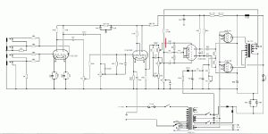
OK. So my amp is based on this schematic with the difference that I have master volume (2x250K pot) after the PI.
So I was thinking the best way to implement the FX loop would be as seen from the attached picture (marked red) right before the phase inverter. Can I just simply cut the wire and solder 1/4" jacks on both sides for my FX loop? I will have to probably attenuate the signal to some guitar level, then buffer it and amplify it before I send it to phase inverter? this is my exact schematic
So I was thinking the best way to implement the FX loop would be as seen from the attached picture (marked red) right before the phase inverter. Can I just simply cut the wire and solder 1/4" jacks on both sides for my FX loop? I will have to probably attenuate the signal to some guitar level, then buffer it and amplify it before I send it to phase inverter? this is my exact schematic
Attachments
Last edited:
If you use ur amp clean, that might work. Tubetown hs a cheap kit for such a loop.
But more likely, you are using ur amp for an overdriven sound, and the Phase Invertor is being overdriven, using a post-phaseinvertor Master Volume to controll the loudness.
In such a case, the FX loopis still pre-clipping and, especially reverd and delay, will sound ugly. You will not be able to add effects after clipping.
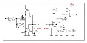
..what is the function of VD1 on this schematic?
It adds 0.6V of bias to the MOSFET. I assume this is correct for this circuit. The suggested diode is only a few pennies so I would not worry about it.
It´s there to bias the first FET, doing essentially the same as the 470 ohm resistor in the second one.I found this schematic online,
can someone tell me what is the function of VD1 on this schematic?
That circuit is extremely odd (and I don't just mean the diode bias.)I found this schematic online
The LND150 on the left is set up with so much negative feedback that it acts as an attenuator, not an amplifier. Why not just use two resistors if all you want is an attenuator? Why use a MOSFET at all?
One good reason to use a MOSFET would have been to buffer the attenuator, so that you had a low send impedance at the FX send jack. This could have been done simply with a source-follower.
But that's not what this circuit does. Instead, the MOSFET is setup as a common-source gain stage, with a very high 100k output impedance at the drain. Then a 220k resistor (R4) heavily loads down this 100k output impedance, throwing away several dB of gain, and bringing the output impedance down to about 68 kilo ohms, still very high. Finally, a lot of negative feedback is applied to bring down the voltage gain of the stage to 0.023x or -33 dB.
Which is just bizarre. Why not use two resistors to divide down the voltage, if attenuation is necessary? A 100k resistor and a 2.2k resistor would provide about the same -33 dB attenuation, and a lower output impedance of 2.2k, all with no MOSFET at all! (Use a 2.2k or 2.5k log pot to take over the send level function of R2.)
That arrangement would have about 100k input resistance. If a higher input impedance is required for some reason, the 100k can be replaced with 470k, and the 2.2k pot can become 10k. About the same attenuation as before, < 10k output impedance, > 470k input impedance. And still no MOSFET needed.
And the silicon diode bias...aye carumba! It is a disastrous idea. MOSFETs have much wider parameter spreads, and much bigger temperature coefficients than vacuum triodes; we know you can successfully bias a 12AX7 with a red LED at each cathode, but this same approach doesn't work reliably with MOSFETs.
Moving on to the FX return side, there is less outright craziness, but trying to "cathode-bias" a MOSFET with a 110k drain resistor and a 470 ohm source resistor is almost as bad as the diode bias on the "send" side - completely unreliable, just begging for trouble really. Slight variations in the LND150 parameters (Vp, Idss) can make the circuit completely non-functional.
For some reason, the majority of online FX loop designs seem to be flawed. Many are very seriously flawed.
I participated in a long thread on FX loops here on diyAudio a year or two ago, which ended happily with the original poster making PCBs and successfully building the FX loop design, which he reported worked well in his guitar amp. Unfortunately, I am completely unable to find that thread using the diyAudio search function.

-Gnobuddy
Thanks for your answer.
I found another schematic online that is pretty much the same as the first one with just a little difference in the first transistor connection.
By reading your post I am scratching my head and thinking to abandon this "two transistor" circuit altogether.
Anyway, here it is:
I found another schematic online that is pretty much the same as the first one with just a little difference in the first transistor connection.
By reading your post I am scratching my head and thinking to abandon this "two transistor" circuit altogether.
Anyway, here it is:
Attachments
Thanks for your answer.
I found another schematic online that is pretty much the same as the first one with just a little difference in the first transistor connection.
By reading your post I am scratching my head and thinking to abandon this "two transistor" circuit altogether.
Anyway, here it is:
Well, your second circuit is way more reasonable
*In general*, loop circuits attenuate signal a lot, since signal at plates can easily reach 90V RMS, and you need about 100/200mV RMS to drive pedals, and then you need to rise that pedal signal again to something between 1V RMS and 5-10V RMS, whatever is needed to drive a Tube power amp, so the *second* gain stage is needed.
The first one? ... not that much, and in general just an attenuator works fine.
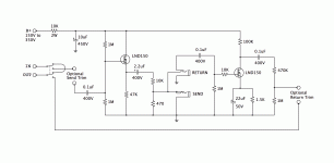
This one is much better!I found another schematic online...
The (left) LND150 is used as a source-follower, properly biased by the two 1 meg resistors. Output impedance at the "send" jack is around 470 ohms, which is nice and low - good!
The "return" circuit is not as well done. Once again the MOSFET uses "self bias", which is not a good idea, because MOSFETs have wide parameter spreads. That means that, in this circuit, some LND150 will work perfectly, some will work badly, some won't work at all.
Also, on the return side, there is nothing to set the voltage gain of the LND150 - no negative feedback at all. This might lead to too much voltage gain here, which means the loop might be noisy (hiss) and may distort unless you turn down the FX pedals volume a lot.
This can easily be fixed, though. Take a look at the attached schematic, which I drew up and simulated in LTSpice for you. This is just the return side, i.e. the right half of the circuit; the left half is fine as it is (the second circuit you posted, the one where the LND150 is biased by the two 1 meg resistors.)
In this circuit, R2/R3 bias the gate of the MOSFET to about +20 volts. This makes the bias stable, and small changes in MOSFET parameters like Vp and Idss will not stop the circuit from working properly any more.
R1 now sets the bias current through the MOSFET at about 1 mA. R4 is 100k as before. But C2 and R5 now control the voltage gain - it is set to about 34 dB or 50x, roughly the same as you would get with one of the triodes in a 12AX7.
C3 (47 pF) is to limit excessive high-frequency response - we don't want our FX loop to pick up AM radio stations!
The value of C4 depends on what you connect this circuit to. You can probably reduce it a lot. For example, if this FX loop output connects to a 1 Meg grid bias resistor of the next valve, then you can reduce C4 to just 0.0047uF (4700pF).
-Gnobuddy
Attachments
Fantastic! Thank you Gnobuddy so much for your time. I appreciate it a lot. I will give this a try and combine with the properly biassed transistor in the first stage. I do have a scope and generator so I can take a peek what is happening before I wire it in. ( I have a clone of JCM 800). I was originally thinking the worst case scenario I would have to buy a handful of LND150, put a socket there and keep swapping one by one until I find the properly working transistor. But your solution is much much better. I now understand what self biasing mean and it would take me long time to figure that out, especially when I go to work and have this as a hobby-time is limited. Thanks again.
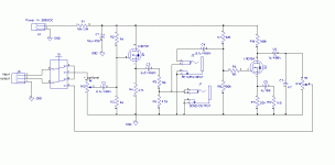
OK, so I re-drew the schematic. I added two 1M trimpots, one on the input and one on the output in case I need to set the proper levels. I also added a by-pass switch. The loop will by-pass on its own through the phone jacks if nothing's plugged into it anyway but the phone jacks' contacts are not always as reliable as we would like, so therefore the DPDT toggle switch to take it out completely.
here it the schematic:
here it the schematic:
Attachments
Glad to help! (DPDT switch looks good!)
I forgot to mention, the 10k resistor (R6) is a "gate-stopper". It's purpose is to stop the MOSFET from self-oscillating. It should be mounted as close to the MOSFET as possible on the PCB.
I think it's a good idea to add a similar 10k resistor to the LND150 on the "send" side of the circuit, as well. It will go between the junction of the two 1 Meg resistors and the gate of the LND150.
If you B+ is reasonably close to 300 volts, it may not need any tweaking, but if it does, drive the FX In jack with the signal generator output at around 300 Hz - 500 Hz, increase the signal level gradually until the output shows clipping on the 'scope, and change R1 (22k) if necessary to get more or less symmetrical clipping at the output.
Please do this without anything connected to the output of the FX loop - it can spit out a huge signal voltage (nearly equal to B+ volts, peak-to-peak), and we don't want this to damage the rest of the guitar amplifier!
An American company called Wampler used to make a guitar pedal called the Wampler Plexi-Drive. It uses 3 JFETs, and tries to sound like a Marshall Plexi. For a pedal, it sounds very good. It is also quite expensive, so people tried to clone it. You can find the schematic online easily.
The trouble is, it doesn't work with 99% of the JFETs that people try! Google will turn up Internet posts from sad people who bought 150 JFETs, tried every single one, and couldn't even find three that worked in this circuit.
The original J201 JFETs are no longer available, but I have a near-substitute, 2N5457. I tried bread-boarding the circuit, and immediately found that all the JFETs I have bias up perfectly - but only if I change the 1k source resistor to 3.3k! With the original 1k, none of my JFETs come anywhere near biasing properly - they are all saturated, fully "on". No wonder people were unable to find any JFETs that worked in this circuit!
I don't know if there is an actual mistake in the reverse-engineered circuit, or whether Brian Wampler originally used some very out-of-spec JFETS that he happened to have. In either case, this is another example where a little bit of electronics theory really helps. With the theory, you can just buy 3 JFETs and they will work. Without it, you can buy 150 JFETs, and even then you may not find 3 good ones!
-Gnobuddy
I forgot to mention, the 10k resistor (R6) is a "gate-stopper". It's purpose is to stop the MOSFET from self-oscillating. It should be mounted as close to the MOSFET as possible on the PCB.
I think it's a good idea to add a similar 10k resistor to the LND150 on the "send" side of the circuit, as well. It will go between the junction of the two 1 Meg resistors and the gate of the LND150.
Excellent! I was guessing at what B+ voltage you had - I designed for 300 volts DC, but if the actual voltage in your JCM clone is different, you (or I) can tweak the design a little if needed.I do have a scope and generator so I can take a peek what is happening before I wire it in.
If you B+ is reasonably close to 300 volts, it may not need any tweaking, but if it does, drive the FX In jack with the signal generator output at around 300 Hz - 500 Hz, increase the signal level gradually until the output shows clipping on the 'scope, and change R1 (22k) if necessary to get more or less symmetrical clipping at the output.
Please do this without anything connected to the output of the FX loop - it can spit out a huge signal voltage (nearly equal to B+ volts, peak-to-peak), and we don't want this to damage the rest of the guitar amplifier!
This might work, but is frustrating, and a waste of your time and money. Also, the MOSFET bias is unstable when the temperature inside the amplifier changes!worst case scenario I would have to buy a handful of LND150, put a socket there and keep swapping one by one
An American company called Wampler used to make a guitar pedal called the Wampler Plexi-Drive. It uses 3 JFETs, and tries to sound like a Marshall Plexi. For a pedal, it sounds very good. It is also quite expensive, so people tried to clone it. You can find the schematic online easily.
The trouble is, it doesn't work with 99% of the JFETs that people try! Google will turn up Internet posts from sad people who bought 150 JFETs, tried every single one, and couldn't even find three that worked in this circuit.
The original J201 JFETs are no longer available, but I have a near-substitute, 2N5457. I tried bread-boarding the circuit, and immediately found that all the JFETs I have bias up perfectly - but only if I change the 1k source resistor to 3.3k! With the original 1k, none of my JFETs come anywhere near biasing properly - they are all saturated, fully "on". No wonder people were unable to find any JFETs that worked in this circuit!
I don't know if there is an actual mistake in the reverse-engineered circuit, or whether Brian Wampler originally used some very out-of-spec JFETS that he happened to have. In either case, this is another example where a little bit of electronics theory really helps. With the theory, you can just buy 3 JFETs and they will work. Without it, you can buy 150 JFETs, and even then you may not find 3 good ones!
-Gnobuddy
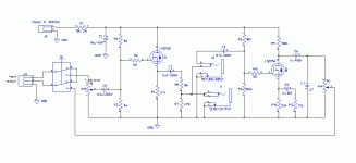
Awesome. Thanks very much once again. Gate stopper resistor added to the first stage. I know gate stopper resistors are a good practice, I learned that from AMB forum but it looks like I need someone to keep reminding me . Yes, I forget stuff...... Since I am not Kim Peek, I guess I am allowed to forget some things in order to put new things to the brain.
new schematic:
. Yes, I forget stuff...... Since I am not Kim Peek, I guess I am allowed to forget some things in order to put new things to the brain. new schematic:
Attachments
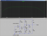
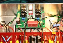
Here are some FX loop updates. I put it all together on affordable PCB . I didn't use any electrolytic caps except the 10uF decoupling cap on power rail. I had to change the first 10K drop down resistor in my amp to 4K7 to compensate for current draw by the FX loop to maintain approximately the same voltages. Power for FX board is tapped from phase inverter that is now 361V feeding the FX board with another 10K resistor that produces 314VDC on C1,R2,Q1,R8,R11. So the current draw by FX board is somewhere around 4.7mA.
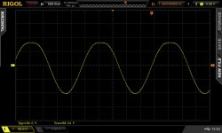
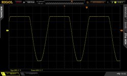
The new re-designed "RETURN" stage that Gnobuddy helped me with has current gain of 46, because I have 1M trimpot on the output not fully open. Feeding 1Vrms from the generator shows 46Vrms on the scope. Voltage clipping happened somewhere around 1.5Vrms input voltage, you can see on scope screen capture.
Input stage transistor Q1 I adjuted by the 1M trimpot R15 on the input roughly to -44x (input 3.43Vrms and 78mVrms voltage drop on R7 resistor), so that the whole loop gain equals 1.
The whole FX loop works very well. No added noise! I do have some uneven clipping as you can see from the picture when the output stage voltage gets very high.
Thank you Gnobuddy for your help.
. I didn't use any electrolytic caps except the 10uF decoupling cap on power rail. I had to change the first 10K drop down resistor in my amp to 4K7 to compensate for current draw by the FX loop to maintain approximately the same voltages. Power for FX board is tapped from phase inverter that is now 361V feeding the FX board with another 10K resistor that produces 314VDC on C1,R2,Q1,R8,R11. So the current draw by FX board is somewhere around 4.7mA. The new re-designed "RETURN" stage that Gnobuddy helped me with has current gain of 46, because I have 1M trimpot on the output not fully open. Feeding 1Vrms from the generator shows 46Vrms on the scope. Voltage clipping happened somewhere around 1.5Vrms input voltage, you can see on scope screen capture.
Input stage transistor Q1 I adjuted by the 1M trimpot R15 on the input roughly to -44x (input 3.43Vrms and 78mVrms voltage drop on R7 resistor), so that the whole loop gain equals 1.
The whole FX loop works very well. No added noise! I do have some uneven clipping as you can see from the picture when the output stage voltage gets very high.
Thank you Gnobuddy for your help.
Attachments
Last edited:
Did you design that PCB and have them made for you? They look great!I put it all together on affordable PCB
I think most of that is on the "send" side. There's about 150V at the FET gate due to the two 1 meg resistors, a volt or two more at the FET source, and a 47k source resistor. So the first FET will draw more than 3 mA of drain current. That means it's also dissipating some 450 - 500 mW, which is quite a lot for such a little FET (TO92 package).So the current draw by FX board is somewhere around 4.7mA.
If I had designed the "send" circuit too, I would probably have increased that 47k source resistor to 100k, just to reduce power dissipation in the LND150 a little bit.
Excellent! I'm happy that it worked out well for you, and glad to have helped a little bit.The whole FX loop works very well. No added noise!
-Gnobuddy
I did the PCB myself using Diptrace and sent it to China to make it happen. The problem is that for through hole parts like Neutrik phone jacks there are no foot prints. So I tried KiCad instead and no foot prints either. So I went back to Diptrace and had to create them.
I was thinking about the heat dissipation on the SEND side myself since there is only 47K resistor and the transistor is biassed half the rail voltage like you wrote, I calculated 0.47W through the resistor (B+ 300V), I used 1W Vishay but forgot about the transistor! I don't care much about the mA draw, I can compensate for that by changing resistors in supply rail, but the heat is certainly concerning. I will have to check that and increase the 47k to 100k like you are suggesting. I was first thinking the higher current might help the low frequencies pass through the large 2u2 capacitor and through the R6, R7 divider, but I didn't dig deeper for any time constants or similar things.
What I will definitely try to do is to make the the return stage more symmetrical. You can see from the picture that the reference 0V line doesn't sit in the middle of the waveform.
Also, I found out that there is a very little low frequency loss (barely noticeable) probably due to C6 and R14. R14 is not all the way up, so it creates frequency roll off when feeding 22nF cap going to phase inverter. I have also seen it on the scope that the shape of the sine wave was changing slightly when adjusting R14, but I realized that later when I was playing my guitar. I must have golden ear.
I have couple of boards left. If someone wants one shoot me a message. Sipping only to US and Canada, no charge.
I was thinking about the heat dissipation on the SEND side myself since there is only 47K resistor and the transistor is biassed half the rail voltage like you wrote, I calculated 0.47W through the resistor (B+ 300V), I used 1W Vishay but forgot about the transistor!
I don't care much about the mA draw, I can compensate for that by changing resistors in supply rail, but the heat is certainly concerning. I will have to check that and increase the 47k to 100k like you are suggesting. I was first thinking the higher current might help the low frequencies pass through the large 2u2 capacitor and through the R6, R7 divider, but I didn't dig deeper for any time constants or similar things. What I will definitely try to do is to make the the return stage more symmetrical. You can see from the picture that the reference 0V line doesn't sit in the middle of the waveform.
Also, I found out that there is a very little low frequency loss (barely noticeable) probably due to C6 and R14. R14 is not all the way up, so it creates frequency roll off when feeding 22nF cap going to phase inverter. I have also seen it on the scope that the shape of the sine wave was changing slightly when adjusting R14, but I realized that later when I was playing my guitar. I must have golden ear
.I have couple of boards left. If someone wants one shoot me a message. Sipping only to US and Canada, no charge.
Last edited:
- Home
- Live Sound
- Instruments and Amps
- Marshall FX loop