So I've been playing around with a Ruby as an electronics learning project, and as an excuse to cut some wood. I've made myself a small fender-ish cabinet that fits baffles for 8" and 10" speakers. To drive this, i etched a Ruby PCB using the storyboardist layout from Perf and PCB Effects Layouts. It worked great for a little while until suddenly it didn't and instead produced a mid-range pitched very intense stable tone that modulated frequency with volume and gain. After some troubleshooting i believe the fault was the J201 JFET (both D and S were close to +9V) and i have a replacement on the way.
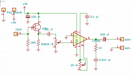
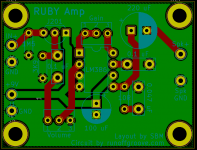
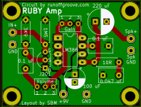
Now, i was a little too fast when making this board and didnt cut the phenolic board large enough to allow for mounting holes. So, thought I, why not call it an excuse to draw up my own layout and have the good folks at DIYaudio school me on it! Having said all this, I hope you will provide me some feedback for this layout. Bear in mind that I am a complete beginner and know pretty much nothing except the bare basics. I am still working out the wrinkles of using KiCad for example, as is probably evident already. I have attached schematic and layout as pictures. The schematic is adapted for the bassman mod (0.1 uf coupling cap from JFET instead of 0.047 uf), and is intended to have pots and other stuff mounted off-board.
Main objective is to have fun and learn something along the way. As for design objectives i'll settle for "works", but i suppose i should say that i loosely copied the storyboardist layout, with a few changes:
- Made it a little less tight to make the component choice less critical.
- Moved 9V+ and PSU gnd inputs to bottom left side
- Double sided. The backside is PSU and a large GND plane. Front is all the signal-related stuff. I don't know if this is the right way to go, but it was easier to route this way...
One question - i notice the noisy cricket has a 220 µf filter cap instead of 100. Does it make sense to increase size or is the benefit academic?
Thanks in advance for your patience and understanding... Pictures of amp cabinet to come!
Attachments
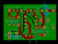
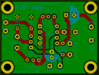
You are lacking a ground return for the input connection, without that you'll have to scrape off the solder-mask to solder the input coax screen to.
I don't see any mounting holes to fix the board to the chassis.
The routing signals one side, power & ground the other is very reasonable.
I don't see any mounting holes to fix the board to the chassis.
The routing signals one side, power & ground the other is very reasonable.
Ok input return pad added.
I would flip the pot connection so the input trace to the pot is more direct.
Last edited:
Thanks rayma, you have sharp eyes and i agree thats better. fixed.
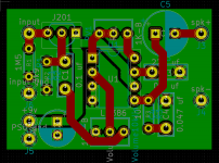
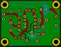
You may not want to do this, but you could exchange the positions of the 100uF (with battery pads),
and the pot connector. At the same time, turn the pot connector 90 degrees. Then reroute the trace
from pin #6 of the amp directly to the 100uF. Leave the trace from the 100uF to the fet where it is.
Last edited:
Hey rayma. I read a few places that the 100 uf cap should be as close as possible to pin 6 of the IC. Am i right that this is the intended improvement and should bring better stability against oscillation?
But in this case, the connection between volume pot and pin 2 of the IC run parallel for some part of the trace (though on opposite sides of the board. Is this acceptable routing or should i try and move one of the traces?
Edit: turned the pot 90 degrees.
Edit edit: d'oh, turning the pot conflicts with the 9v trace. back again...
Attachments
Last edited:
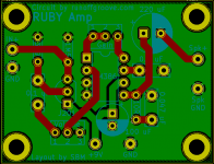
Ok a little further now, silkscreen text updated. Still room for changes of course. I am still unsure whether the parallel traces between volume pot pin 2 and IC pin 2 and V+ are OK...
I also noticed there is a protection diode between 9V+ and GND on the storyboardist layout. Am i right that this is simply to protect from accidentally reversing polarity of the power supply?
I also noticed there is a protection diode between 9V+ and GND on the storyboardist layout. Am i right that this is simply to protect from accidentally reversing polarity of the power supply?
Attachments
I am still unsure whether the parallel traces between volume pot pin 2 and IC pin 2 and V+ are OK... Am i right that this is simply to protect from accidentally reversing polarity of the power supply?
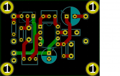
The input and 9V traces should be ok.
It would work out better if the battery pads were below the 100uF.
Yes, you don't really need the diode.
How about this?
Looks good. I'd still have the volume control pin 2 trace go up, instead of
wrapping around the bottom first.
I'd reverse the two battery pads, so there's more ground plane area between
the 100uF negative pad and the speaker minus pad.
Last edited:
Thanks rayma I will implement your suggestions ASAP. The kids have taken over the PC to watch a film so will be a little bit ")
I am not totally sure I understand what you mean. Reversing the battery pads, I assume you mean switch +9V onto left side and gnd to right. Not sure what you mean by more gnd plane between 100uf and speaker - though...
I am not totally sure I understand what you mean. Reversing the battery pads, I assume you mean switch +9V onto left side and gnd to right. Not sure what you mean by more gnd plane between 100uf and speaker - though...
Last edited:
Reversing the battery pads, I assume you mean switch +9V onto left side and gnd to right.
Not sure what you mean by more gnd plane between 100uf and speaker - though...
The pot trace doesn't have to be so wide, if that helps.
The return current from the speaker flows back through the ground plane
and to the negative end of the 100uF capacitor. If you reverse the battery pads,
the trace from the positive battery pad won't obstruct the ground plane so much.
Ok i get it now. Here's another try.
Looks good. I would move the trace from the output terminal farther from the mounting hole.
Now check all the footprints again for correct hole sizes and spacing.
I will go through the footprints next and double check against the parts i've got. .
Believe me, you can overlook an error ten times and just not see it.
Check the mounting holes, too.
Ok so i went through and found that footprints for resistors and caps were too small. Updated them to correct size and everything still fits. So far so good!
Good catch. There may not be enough clearance room at the ends of the IC (or socket)
for the 100uF and the gain pot. Some ICs will go beyond the end of the socket.
Last edited:
- Status
- This old topic is closed. If you want to reopen this topic, contact a moderator using the "Report Post" button.
- Home
- Live Sound
- Instruments and Amps
- 2-sided board for Ruby Amp