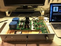
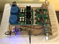
After a couple of months of development, I got this up and running tonight. Sounds pretty good in comparison to my DCG3. If there is any interest, I can follow up with more details.
Attachments
Last edited:
Sure, thanks for asking.
Over the winter, I decided to build Salas' DCG3. I designed a PC board roughly following the official layout, and also designed a power supply board based on the Super Regulator schematic. This was my first experience with "real" headphone systems. It came out really well and I ended up building another, which I sold to a friend. He described it as "The best headphone amplifier I have heard," which is a testament to Salas' design skill more than my construction ability.
After finishing those projects, I was reading the Wolverine amplifier thread on the solid-state forum, and also reading Douglas Self's book. The DCG3 circuit is relatively simple for a discrete op-amp. I started wondering whether adding more bells and whistles to the circuit would make things better, worse, or indifferent. The goal was to try something very conventional and boring as a reference point for future projects that might be more original.
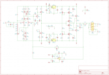
What I came up with is a standard Blameless front end mated to a Class A diamond buffer output stage. I cribbed Salas' DC servo circuit from the DCG3 and powered it with another copy of my Super Regulator board.
I have a delay circuit I designed that operates the DCG3 muting relay and also switches a bi-color power indicator LED. I didn't have parts to make one of these, so I decided just to run the relays with a battery and a switch. Unfortunately, the switch I bought Saturday turned out to be momentary contact, so I have to wait until Monday to buy a new one.
I will follow up with more information in a second post.
Over the winter, I decided to build Salas' DCG3. I designed a PC board roughly following the official layout, and also designed a power supply board based on the Super Regulator schematic. This was my first experience with "real" headphone systems. It came out really well and I ended up building another, which I sold to a friend. He described it as "The best headphone amplifier I have heard," which is a testament to Salas' design skill more than my construction ability.
After finishing those projects, I was reading the Wolverine amplifier thread on the solid-state forum, and also reading Douglas Self's book. The DCG3 circuit is relatively simple for a discrete op-amp. I started wondering whether adding more bells and whistles to the circuit would make things better, worse, or indifferent. The goal was to try something very conventional and boring as a reference point for future projects that might be more original.
What I came up with is a standard Blameless front end mated to a Class A diamond buffer output stage. I cribbed Salas' DC servo circuit from the DCG3 and powered it with another copy of my Super Regulator board.
I have a delay circuit I designed that operates the DCG3 muting relay and also switches a bi-color power indicator LED. I didn't have parts to make one of these, so I decided just to run the relays with a battery and a switch. Unfortunately, the switch I bought Saturday turned out to be momentary contact, so I have to wait until Monday to buy a new one.
I will follow up with more information in a second post.
Attachments
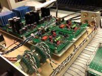
The circuit is self-explanatory, but here are a few notes.
I've had some National 2N556s in my junk box for forty years and designed this circuit to use them. The LSK389 in a TO-71 can is pin compatible and you can actually buy them. It would probably work well in this circuit, with less noise.
I scrounged genuine BC549Cs, BC550Cs, and BC560Cs from various places, but getting devices could be a problem for anyone wishing to duplicate this circuit. I have been working on an SMD layout which shows promise. But I'm kinda running out of steam so don't have an immediate plan to finish that project.
I added an active cascode to the front end. I decided to use cascode current sources instead of the more popular ring-of-two. The rationale is to avoid the global feedback of the ring-of-two. The prototype had a cascode current source for the VAS also, but I simplified it in the interest of getting more symmetrical clipping.
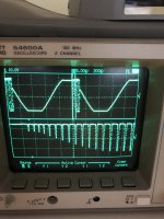
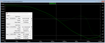
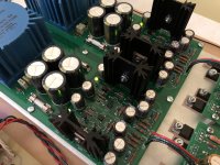
Another change from the prototype was removing the VAS active current limiter and replacing it with a Schottky Baker clamp diode. As you can see in the picture, there was a severe stability problem with the current limiter coming out of clipping on positive peaks. Clipping is clean now, with just a bit of rail sticking evident on both positive and negative peaks.
I don't have SPICE graphs handy, but I can post them later. SPICE shows loop gain of around 125dB at DC, with 70 dB of loop gain at 20kHz. With so much gain, I opted for pretty heavy input stage degeneration. Simulated unity gain crossover is around 10 MHz, phase margin around 60 degrees, and gain margin around 10 dB. I used two-pole compensation, evidently. I haven't seen any indication of instability, which was not the case for my version of the DCG3.
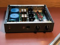
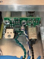
The output stage bias is about 160 mA. The TO-126 drivers are cross-coupled and dissipate very little power. I chose them so I could bolt them to the heat sink for thermal compensation. The output stage bias has a slight negative tempco, which is good. Heatsinking is marginal but adequate with this prototype. It's dissipating about 5W total in that metal plate and is just on the hairy edge of painfully hot to the touch.
I was going to use capacitance multipliers to isolate the driver power supplies, but LDOs were easier to lay out. I was concerned about noise, both from the LDOs and the 2N5564 inputs (which aren't as quiet as 2SK389s), but the amplifier is dead quiet.
The power supply grounds are independent and floating. The 220uF rail filter caps are sitting on a local ground which is isolated from the driver stage ground via a 10 Ohm resistor. I run separate wires for the "dirty" output and "clean" input grounds to the common terminal strip near the headphone jack. There are a couple of unavoidable current loops in this design, but the 10 Ohm resistors seem to be doing their jobs.
With the DC servos, output offset is on the order of 10 uV, within the margin of error of my Fluke 287 DMM.
I've had some National 2N556s in my junk box for forty years and designed this circuit to use them. The LSK389 in a TO-71 can is pin compatible and you can actually buy them. It would probably work well in this circuit, with less noise.
I scrounged genuine BC549Cs, BC550Cs, and BC560Cs from various places, but getting devices could be a problem for anyone wishing to duplicate this circuit. I have been working on an SMD layout which shows promise. But I'm kinda running out of steam so don't have an immediate plan to finish that project.
I added an active cascode to the front end. I decided to use cascode current sources instead of the more popular ring-of-two. The rationale is to avoid the global feedback of the ring-of-two. The prototype had a cascode current source for the VAS also, but I simplified it in the interest of getting more symmetrical clipping.
Another change from the prototype was removing the VAS active current limiter and replacing it with a Schottky Baker clamp diode. As you can see in the picture, there was a severe stability problem with the current limiter coming out of clipping on positive peaks. Clipping is clean now, with just a bit of rail sticking evident on both positive and negative peaks.
I don't have SPICE graphs handy, but I can post them later. SPICE shows loop gain of around 125dB at DC, with 70 dB of loop gain at 20kHz. With so much gain, I opted for pretty heavy input stage degeneration. Simulated unity gain crossover is around 10 MHz, phase margin around 60 degrees, and gain margin around 10 dB. I used two-pole compensation, evidently. I haven't seen any indication of instability, which was not the case for my version of the DCG3.
The output stage bias is about 160 mA. The TO-126 drivers are cross-coupled and dissipate very little power. I chose them so I could bolt them to the heat sink for thermal compensation. The output stage bias has a slight negative tempco, which is good. Heatsinking is marginal but adequate with this prototype. It's dissipating about 5W total in that metal plate and is just on the hairy edge of painfully hot to the touch.
I was going to use capacitance multipliers to isolate the driver power supplies, but LDOs were easier to lay out. I was concerned about noise, both from the LDOs and the 2N5564 inputs (which aren't as quiet as 2SK389s), but the amplifier is dead quiet.
The power supply grounds are independent and floating. The 220uF rail filter caps are sitting on a local ground which is isolated from the driver stage ground via a 10 Ohm resistor. I run separate wires for the "dirty" output and "clean" input grounds to the common terminal strip near the headphone jack. There are a couple of unavoidable current loops in this design, but the 10 Ohm resistors seem to be doing their jobs.
With the DC servos, output offset is on the order of 10 uV, within the margin of error of my Fluke 287 DMM.
Attachments
Finally, sound quality. I was very surprised and impressed that I just turned the thing on and it sounded great from the get-go with no futzing around to get rid of hum and buzz.
I auditioned with my Sennheiser HD560S. I don't have golden ears and I'm not sure I could tell the difference between this amp and the DCG3. Both of them have a big, effortless sound with seemingly very good resolution. The new amp is very detailed but not at all etched that I can tell. It actually sounds "warm," whatever that means. I interpret that as meaning there's a lack of IMD.
I will try to find an audiophile friend with listening talent to audition the amp and give his assessment.
This is a pretty complicated design, with 21 transistors per channel versus the DCG3s eight. I did it mainly as a technical exercise. Still, if anyone is interested in trying to duplicate it, I have three left-over boards here, and I can share the PC design files.
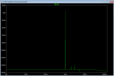
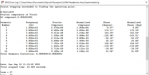
Here's the SPICE data. I remembered wrong about the GBW; it's only 2.3 MHz, but still sufficient. I don't trust SPICE distortion simulations, so take that with a grain of salt. The simulation is with 6V pk-pk into a 12 Ohm load. With a less demanding load, the distortion vanishes from the graph, FWIW.
Attachments
Last edited:
You're right, you found a typo on the schematic. Thanks, I'll fix it.
I use the Semitech CRDs from Mouser. Everything is tightly regulated, but it occurred to me I could put a CRD in the same space as a resistor and get better PSRR from my current sources. I could probably use the CRDs by themselves, or in cascode, instead of the LED-biased transistors. But the data sheet says they're not tightly specified for set current, so I did it this way.
I've deliberately downplayed the subjective angle but maybe I should promote this design a little. I spent a few hours listening to it over the weekend and I think it's a phenomenal sounding amplifier. I was thrilled with the sound of the DCG3 when I got it running, and I think the new amplifier is better. It's hard or impossible to make subjective claims as matter of fact. But I have a strong sense that the new amp just sounds more lifelike. Sometimes it really startles me, actually, in a way that didn't happen before.
Obviously, I'm biased so I want to let some other people listen and give me their impressions.
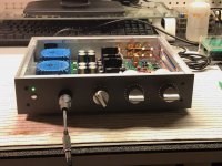
The 9V batteries don't last very long and are expensive. So I've been working today on a timer circuit. This is tested and ready to install later today.
I use the Semitech CRDs from Mouser. Everything is tightly regulated, but it occurred to me I could put a CRD in the same space as a resistor and get better PSRR from my current sources. I could probably use the CRDs by themselves, or in cascode, instead of the LED-biased transistors. But the data sheet says they're not tightly specified for set current, so I did it this way.
I've deliberately downplayed the subjective angle but maybe I should promote this design a little. I spent a few hours listening to it over the weekend and I think it's a phenomenal sounding amplifier. I was thrilled with the sound of the DCG3 when I got it running, and I think the new amplifier is better. It's hard or impossible to make subjective claims as matter of fact. But I have a strong sense that the new amp just sounds more lifelike. Sometimes it really startles me, actually, in a way that didn't happen before.
Obviously, I'm biased so I want to let some other people listen and give me their impressions.
The 9V batteries don't last very long and are expensive. So I've been working today on a timer circuit. This is tested and ready to install later today.
Attachments
Could you show us how the psu pcb is drawn? Looks like a very well thoughtout mix of trace & plane ground and id like to take notes and learn from it if i can.
Also i wholeheartedly endore the overall layout which is the same as the yarra preamp and also mine that i plan on documenting here near future. When its all been considered and compromised, the way yours is now, is really the best solution for a one chassis dual mono layout.
Also i wholeheartedly endore the overall layout which is the same as the yarra preamp and also mine that i plan on documenting here near future. When its all been considered and compromised, the way yours is now, is really the best solution for a one chassis dual mono layout.
To me the good part is keeping the input and the volume farthest away from the tranformer and also the input wiring spaced away from any active circuitry. Mine that follows this same layout is a modular preamp and on it ive also tweaked the module pins such a way that not even any power and signal traces cross eachother on the board. (Made possible thru the gap provided by the unavoidable elevation of the module pcb). The result is a dead quiet output. Lower than average noise floor that can definitely be appreciated by experienced ears when compared to a run of the mill product. Im sure yarra has that same positive trait and this headphone amp too. They are just very well designed projects.
Thanks for the comments. I try to learn and copy good designs when I see them.
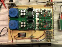
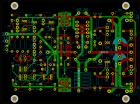
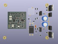
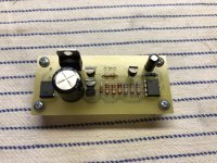
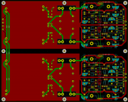
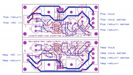
Here's the power supply layout. It's close to Jan Didden's board. I left out the remote sensing connections and set up a common ground bus per channel. This seems to work well.
The three-wire output jack forces a common ground at that point and I decided to connect from there to the chassis plate. There will be a ground loop through the shields of the input cables. It might be better to tie the input jack grounds together to keep the loop inside the chassis. There's no perfect solution.
The voltage drop across the ground wires from the boards to the headphone jack will drive some tiny current through the 10 Ohm isolation resistors into the local star grounds. The alternative was to run even more ground wires around the chassis. I decided not to worry about it.
I was really surprised that I didn't have to fool with anything to make the amplifier quiet. I hear nothing with the volume all the way up when I listen with some some sensitive headphones I use for testing.
I lad out my own PC board for the DCG3 and used matched LSK170s instead of the monolithic LSK389s specified on the schematic. I also used the same Super Regulator power supply instead of Salas' regulator. So my DCG3 should sound similar, but not identical, to the official design. With that caveat, after more listening, I'm still feeling like this new amplifier is incrementally better than the DCG3.
Attachments
I was also noting the similarity with the Yarra dual mono PSU.")
Nice boards. I don't recall reading about this design. I'll look it up.
I think Talema must be struggling with COVID because many of their encapsulated transformers are out of stock at Digi-Key. I lucked out and found the same 15-0-15V transformers with RS labeling on the RS Exports website in England. They were actually cheaper than Digi-Key and arrived in the same amount of time. But the other day I got an email from RS Exports saying they won't do any more business with me until I supply them with a tax exemption certificate.
To me the good part is keeping the input and the volume farthest away from the tranformer and also the input wiring spaced away from any active circuitry. Mine that follows this same layout is a modular preamp and on it ive also tweaked the module pins such a way that not even any power and signal traces cross eachother on the board. (Made possible thru the gap provided by the unavoidable elevation of the module pcb). The result is a dead quiet output. Lower than average noise floor that can definitely be appreciated by experienced ears when compared to a run of the mill product. Im sure yarra has that same positive trait and this headphone amp too. They are just very well designed projects.
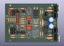
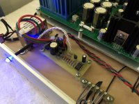
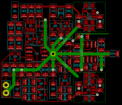
The main things I tried to do with the amp PCB layout are to minimize the loop area around the rail capacitors and output devices in the output stage, and implement an isolated star ground in the input stage. Otherwise, I just spent many, many hours staring at and refining the layout. I'm pretty satisfied with it now.
I've attached the current state of my SMD version of the board. This was a really challenging job for me. It's kind of insane and I'm not sure I'll ever go ahead and build it. If I do, I'll probably ditch the discrete output stage and use an LME49600 just to keep the size down.
It isn't clear that any of this sounds better than a two-chip integrated design. But we do it for the mental exercise, right?
Attachments
Nah, I found an even better way to do it that's cheaper, smaller, uses less power, and has lower distortion.
Edit: Didn't mean to dismiss your suggestion. It would be interesting to see how tiny I could make the circuit. I don't think I need to reduce loop areas for performance, though. It's amazing how they used to make hi-fi equipment without SMD parts, remember?
Edit: Didn't mean to dismiss your suggestion. It would be interesting to see how tiny I could make the circuit. I don't think I need to reduce loop areas for performance, though. It's amazing how they used to make hi-fi equipment without SMD parts, remember?
Attachments
Last edited:
Once again wonderful layout, hpasternack. And yes when the level of effort is high enough it can begin to feel like an artwork, much like yours, and thats why we do it.
Interesting how the ground plane overlaps the ac traces. Ive been told not to do that but if its how jan fid then no need to doubt it
Interesting how the ground plane overlaps the ac traces. Ive been told not to do that but if its how jan fid then no need to doubt it
Interesting how the ground plane overlaps the ac traces. Ive been told not to do that but if its how jan fid then no need to doubt it
I'm not sure if you're talking about the AC power wiring overlapping the ground plane on the left side of the board, or a general rule about avoiding coupling between ground and signal traces.
The official Super Regulator board doesn't include the raw supply. You can see I copied the layout pretty freely.
It could be that extending the ground plane on my board over the transformer primary wiring could allow some injection of AC mains noise into the signal ground. On the other hand, whatever coupling there is, it's likely to be even greater between the primary and secondary windings inside the power transformers themselves.
I reasoned at the time that the ground plane might reduce EMI from the transformers and rectifiers. But ground currents always have to go somewhere and they can cause trouble along the way. I'll have to think about that. Thanks for the observation.
Attachments
- Home
- Amplifiers
- Headphone Systems
- New Headphone Amplifier Design