I've changed the op amp to a OPA1652 and added a gain switch and now I'm thinking of decreasing the value of the emitter resistors and removing the negative feedback capacitor.
I know that decreasing the emitter resistors too much leads to thermal runaway because it increases idle current, but how much can I decrease them by before that starts to be an issue?
As for the feedback capacitor, I simulated it in LTspice (5R emitters) and it appears to still be stable even without it.

Removing the gain resistor also appears to not trouble the circuit at all, so I plan to use two gain levels of x1 gain and x6.1 gain with a 5k1 resistor.

Are any of these things a bad idea? Please advise!
I know that decreasing the emitter resistors too much leads to thermal runaway because it increases idle current, but how much can I decrease them by before that starts to be an issue?
As for the feedback capacitor, I simulated it in LTspice (5R emitters) and it appears to still be stable even without it.
Removing the gain resistor also appears to not trouble the circuit at all, so I plan to use two gain levels of x1 gain and x6.1 gain with a 5k1 resistor.
Are any of these things a bad idea? Please advise!
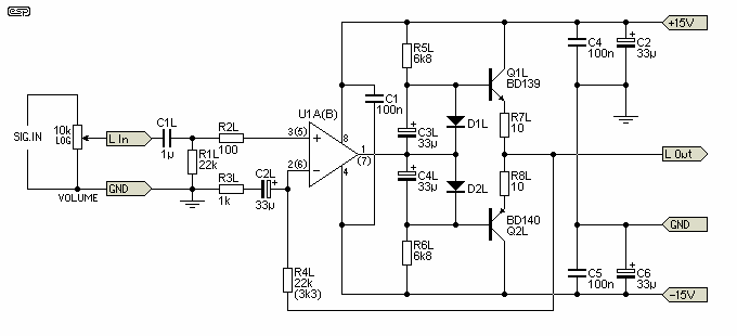
After a lot of playing around in LTspice, I figured out that two series biasing 1N4148s, R5/R6 at 3k3 and R7/R8 at 7R5 would let me bias the output state at more or less Class A until 12Vpp (where I plan to let the amp max out with x6.0 gain). With MJE15028/29/30/31s, Vout being 8.4852Vrms and Ic being 114.59mArms, the transistors need to dissipate 0.97Wrms which should be easily doable. THD is also very much adequate especially for such a simple design, and output power is 2.25W, way more than I'll ever need.


Last edited:
I´m not an expert for LTspice nor composite amplifiers but I don´t think you can trust those THD values.
I´d guess that, PCB design assumed to be flawless, the THD figures will be much better (in the original case/circuit) due to the composite arrangement (depending on the controlling opamp to a large extent).
I´d guess that, PCB design assumed to be flawless, the THD figures will be much better (in the original case/circuit) due to the composite arrangement (depending on the controlling opamp to a large extent).
Yeah I'm aware it's just an approximation, I'm more looking at whether it's functional and not completely broken.
It's just a standard opamp voltage gain stage followed by a complementary BJT current gain stage with diode bias so it shouldn't perform too terribly once laid out on a board.
To be quite honest though, I'm still not sure what those electrolytic caps paralleled with the diodes do.
It's just a standard opamp voltage gain stage followed by a complementary BJT current gain stage with diode bias so it shouldn't perform too terribly once laid out on a board.
To be quite honest though, I'm still not sure what those electrolytic caps paralleled with the diodes do.
There is a difference between 1. an opamp gain stage with its own local feedback + following a separate current buffer and 2. a composite amplifier where the feedback is taken from the output stage.It's just a standard opamp voltage gain stage followed by a complementary BJT current gain stage with diode bias so it shouldn't perform too terribly once laid out on a board.
Yeah I'm aware it's just an approximation, I'm more looking at whether it's functional and not completely broken.
Then you should me more worried about stability into different loads imo. Says on your profile you are currently a university student like myself. Did you already have a lecture on system and control theory? I don't know the best publications in english language on the subject, but you could search for Sergio Franco if you want something very focussed on OpAmp applications. His book "Design with Operational Amplifiers" has a chapter on stability and he has also published some articles here: https://www.edn.com/author/sergio-franco/
Searching for "composite amplifier stability" on your favourite search engine should also bring up quite a bunch of app notes from different manufacturers. You can pour a lot of time into this, depending if you are after a general understanding of system and control theory or if you just want your headphone amplifier design to work.
Another helpful link is this one: Frank Wiedmann - Loop Gain Simulation
Of course you do not always have to study every circuit to the fullest before you build it but it´s good to understand the basics at least (and it is an opportunity to learn and maybe even have more fun)
In this case you are dealing with a composite amp and possible instability so either you are able to verify stability or stay very close to the recommendations/parts given. (though it is generally recommended to check stability, expected current draw etc.)
I built the "original" with a NE5534 and the performance was stellar.
Also notice the different biasing with the LED.
Build This High Quality Headphone Amplifier. – HeadWize Memorial
Last edited:
I actually did experiment with using LEDs to bias the circuit, I know red LEDs are exceptionally quiet parts.
Indeed, that's a very similar circuit, and they also use that small capacitance cap between opamp input and output like I mentioned I thought about earlier.
I'm new to amp design so I intend to check the basics qt least to make sure everything is functional. I'm definitely having fun doing this too, and I can't wait to actually build this circuit in real life.
Last edited:
That´s miller compensation and is one of many compensation techniques used in composite amplifier designs. (dominant pole compensation, lead/lag-compensation you will see most often)they also use that small capacitance cap between opamp input and output
I´m sure you will like the amp!can't wait to actually build this circuit in real life
Just realized I forgot to answer your uni question. Only a first year student here, got through the basic maths and physics courses, nothing specialized yet.

I also tried the LED bias method again, this time with some proper 1.7V red LED models, and I've decided to stick with it. Performs more than well enough for my requirements and I'm always down to use less parts.

By the way, what are C3 and C4 for? Still haven't worked it out.
Edit:
Using bias LEDs have of course resulted in much higher Ic so emitters are going back to 10R. Still results in 1.18W/transistor which is more than before, and 2.59W output power.

Ah, makes a lot of sense. Only 22pF was enough to make the amp stable with a 1uF in parallel with the 32R load, quite amazing stuff. (Yes R5 is 2k2, forgot to change it heh).That´s miller compensation and is one of many compensation techniques used in composite amplifier designs. (dominant pole compensation, lead/lag-compensation you will see most often)
I also tried the LED bias method again, this time with some proper 1.7V red LED models, and I've decided to stick with it. Performs more than well enough for my requirements and I'm always down to use less parts.
I hope so! I've put quite a lot of hours into it nowI´m sure you will like the amp!
By the way, what are C3 and C4 for? Still haven't worked it out.
Edit:
Using bias LEDs have of course resulted in much higher Ic so emitters are going back to 10R. Still results in 1.18W/transistor which is more than before, and 2.59W output power.
Last edited:
They couple the signal to the base of the transistors and stabilize bias voltages.By the way, what are C3 and C4 for? Still haven't worked it out.
It´s nice to see those things working right? It is also very educational when you start doing AC-analyses with LTspice and look at the bode plots.Ah, makes a lot of sense. Only 22pF was enough to make the amp stable with a 1uF in parallel with the 32R load, quite amazing stuff.
(keywords: open loop gain, closed-loop-gain, tian-probe; see links from knoppers)
But keep in mind that the opamp-model is not close to reality!
So the OPA1652 will behave very differently!
(just like the 0.1uF caps next to your voltage sources don´t do much other than being charged because they are connected to a (unrealistic) ideal voltage source)
A composite amplifier is also not a good place to start rolling opamps.
If I were you I´d stick with one of the original circuits. (meaning same bias, same opamp; same everything actually and go from there if you like)
I haven´t simulated that circuit but I don´t think you´ll ever need a LED instead of 1xdiode (2.1V instead of 0.6V). 30mA bias current through the transistors should be plenty. The Earle Eaton amp is different, it uses 1x LED for both base-emitter-junctions.
If you are doing your PCB, you could put 2 diodes in your schematic instead of one. Bridge one at first and you can "hotrod" your circuit later and install the second. (though I´d guess that you won´t need it)
Last edited:
I think SPICE can be educational if you know what to expect and why, so you can actually interpret the simulation results. Otherwise you quickly end up chasing ghosts in a haunted castle. Also the models can be quite accurate, depending on what parameters we are talking about. But one must always remember the assumptions made, the limitations of models and simulation in general, the spread of parameters in the real world, layout parasitics etc.
About the simulation: You can't use 1kHz sinewave and a closed loop for loop stability analysis. Also 100nF is very unrealistic. I would stick with stepping the capacitance in the range from 100pF to a maximum of 10nF. Even the 10nF already represent spools full of cable.
About the simulation: You can't use 1kHz sinewave and a closed loop for loop stability analysis. Also 100nF is very unrealistic. I would stick with stepping the capacitance in the range from 100pF to a maximum of 10nF. Even the 10nF already represent spools full of cable.
Last edited:
Makes sense.They couple the signal to the base of the transistors and stabilize bias voltages.
I did start from there in LTspice, and then I wanted to see what would happen if I increased the bias current, and then here I am. What a journeyIt´s nice to see those things working right? It is also very educational when you start doing AC-analyses with LTspice and look at the bode plots.
(keywords: open loop gain, closed-loop-gain, tian-probe; see links from knoppers)
But keep in mind that the opamp-model is not close to reality!
So the OPA1652 will behave very differently!
(just like the 0.1uF caps next to your voltage sources don´t do much other than being charged because they are connected to a (unrealistic) ideal voltage source)
A composite amplifier is also not a good place to start rolling opamps.
If I were you I´d stick with one of the original circuits. (meaning same bias, same opamp; same everything actually and go from there if you like)
I'm deliberately trying to bias the circuit in class A so that's why I'm using the LEDs instead of diodesI haven´t simulated that circuit but I don´t think you´ll ever need a LED instead of 1xdiode (2.1V instead of 0.6V). 30mA bias current through the transistors should be plenty. The Earle Eaton amp is different, it uses 1x LED for both base-emitter-junctions.
If you are doing your PCB, you could put 2 diodes in your schematic instead of one. Bridge one at first and you can "hotrod" your circuit later and install the second. (though I´d guess that you won´t need it)
You're right really, I also used square waves and varied the capacitance too. I just wanted to see what worst-case was. Not sure how to do analysis without the closed loop though, how would I go about this?About the simulation: You can't use 1kHz sinewave and a closed loop for loop stability analysis. Also 100nF is very unrealistic. I would stick with stepping the capacitance in the range from 100pF to a maximum of 10nF. Even the 10nF already represent spools full of cable.
I gotta say, PCB layout is my forte, not circuit design. This is fun though!
Edit: now that I think about it, I already did AC analysis:

Doesn't really show my modifications were detrimental though cause the original circuit was this:

Last edited:
I think the composite arrangement of these amps will result in a much lower THD than the bias currents alone would suggest.I'm deliberately trying to bias the circuit in class A so that's why I'm using the LEDs instead of diodes
Would love to see THD measurements between the standard version and one with higher bias. Don´t think the difference will be worth it.
If you want pure Class-A with good sound for pennys, you could try this one:
(I´m sure it "breadboards" just fine)
3 Transistor HP Amplifier with low dist
- Home
- Amplifiers
- Headphone Systems
- ESP P113 Modifications