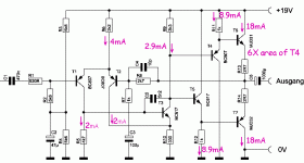
I want to present a re-engineered circuit of a professional headphone amp. There was no documentation therefore i had to get the circuit from the double sided printed board with smd on the upper side. Unfortunately, the bottom of the board was not accessible, but I could measure the missing connections. The circuit is attached as a PDF (project_kh.pdf). Let me say it's not my invention so I don't own the copyright. I double checked the circuit as it is very strange in some parts.
I checked the quality of the amplifier using RMAA, have attached the very good measurement results as a PDF. It's the Project Head Box 2 DT990 Pro file, the other file (Corda Jazz) was uploaded by accident and I can't delete it...
What I don't understand at all is the output stage, which is a pure class B with nearly no quiescent current, but it has a driver stage class A in front of it where 18 mA current are wasted. What is the advantage of this design?
What makes me very curious is the feedback from the VAS stage to the input stage via resistor R10 to transistor T2. I've never seen such a combination. Any ideas?
Heinrich
Attachments
9mA in driver!
T6 is six times bigger than T4 (3A vs 500mA). 2 or 3 octaves. At same current we expect very roughly 50mV difference. It won't be same current but perhaps not far off. 50mV in 2.7 Ohms is 18mA in T6. Eyeballing the ON Semi plots also gives a number somewhat around 20mA.
T6 is six times bigger than T4 (3A vs 500mA). 2 or 3 octaves. At same current we expect very roughly 50mV difference. It won't be same current but perhaps not far off. 50mV in 2.7 Ohms is 18mA in T6. Eyeballing the ON Semi plots also gives a number somewhat around 20mA.
Attachments
Last edited:
This model amplifier must have been redesigned at some point - what was posted here was another circuit altogether!
I wouldn't exactly call this one state of the art but it should work alright - loop gain is sort of limited but as long as it's all in Class A, distortion should remain decently low. Probably not a slew rate king.
I wouldn't exactly call this one state of the art but it should work alright - loop gain is sort of limited but as long as it's all in Class A, distortion should remain decently low. Probably not a slew rate king.
I have revised the circuit again. R10 was a misprint, the resistance is only 33 ohms. I measured the capacitors again, with very short wires and a professional RLC meter, the values are now more realistic.
I also borrowed a professional multimeter. The emitter resistances of the emitter follower output stage transistors have a nominal value of 2.2 ohms (microscope required) and actually are closer to 2.0 ohms. This means that this is a class A power amplifier with a quiescent current of around 7 mA (which I didn't understand previously).
However, the measurements also showed that the differential amplifier at the input is quite unbalanced. Funny that you still get a good harmonic distortion. Maybe it's the current feedback from the VAS stage?
Heinrich
Attachments
It is a version of the so-called Lender circuit.What makes me very curious is the feedback from the VAS stage to the input stage via resistor R10 to transistor T2. I've never seen such a combination. Any ideas?
"4.7k" might be 470? (I'm having trouble matching part numbers to the photograph.)
I've checked it again, it's nominal value is 4.7 kOhms (472 on it) and the real value is 4.62 kOhms, measured with a professional meter on both channels.
Heinrich
In the meantime I tried the analysis of the LTP-VAS part of the circuit with the help of LTSpice. I reduced the capacitors from 470 p to values which are more familiar for me though.
Regardless wether the collector of the second LTP Transistor was connected to ground or to the emitter degeneration resistor of the VAS transistor I got nearly the same values for THD. Maybe I made an error as the values are generally 10 times higher as measured with RMAA at the real unit. Would be very glad if someone can look over the simulation.
Heinrich
Attachments
- Status
- This old topic is closed. If you want to reopen this topic, contact a moderator using the "Report Post" button.
- Home
- Amplifiers
- Headphone Systems
- Let's discuss a professional circuit