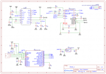
RIGHTINP and RIGHTINM of the TPA6130A2 are both connected to same output of DAC...
Good eye on that. The ES9023 outputs single ended, so the idea is to run the TPA6130A2 as a non-inverting single ended in, single ended out amplifier since there's no point of converting a single ended output (on the dac) to a differential to go to the amp, then get converted back again to single ended.
Thanks for the point out, I'll get that fixed
")
Kaden
Re-check the DAC datasheet again.
Ground connection should not connect this way. Also the DAC output why there cap to ground?
Vreg short to AVcc?
I uploaded both the datasheet example and my schematic. They seem to be pretty similar but maybe I made a mistake in the schematic.
This DAC is a voltage-output DAC, so it there will be a little bit of DC voltage. The caps are AC-coupling capacitors to block the DC voltage.
Kaden
Attachments
Here's the complete datasheet:
https://www.mouser.com/datasheet/2/1082/ESS_11162020_ES9023_Datasheet_v0_71-1923637.pdf
It mentions separating digital and analog ground for the charge-pump.
Kaden
https://www.mouser.com/datasheet/2/1082/ESS_11162020_ES9023_Datasheet_v0_71-1923637.pdf
It mentions separating digital and analog ground for the charge-pump.
Kaden
I only looked at the amp.
https://www.ti.com/lit/ds/symlink/tpa6130a2.pdf
just copy the layout and done.
A bit of action to find 16 ohm headphones, the Mackie only
usually only DJ models are 35-100 ohm, HiFi go up to 600
Anyway for high end not interesting
https://www.ti.com/lit/ds/symlink/tpa6130a2.pdf
just copy the layout and done.
A bit of action to find 16 ohm headphones, the Mackie only
usually only DJ models are 35-100 ohm, HiFi go up to 600
Anyway for high end not interesting
Ok.
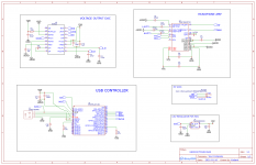
So for the Vreg, do follow the datasheet with 2 resistor.
Unmount the one that connects to supply.
You may still want to short both Agnd and Gnd somewhere on the board using resistor.
I recommend using 0 ohm resistor at you star ground. If don't need still can be remove.
So for the Vreg, do follow the datasheet with 2 resistor.
Unmount the one that connects to supply.
You may still want to short both Agnd and Gnd somewhere on the board using resistor.
I recommend using 0 ohm resistor at you star ground. If don't need still can be remove.
The TPA6130 is BGA or QFN only. That will be a bit of a challenge to solder. I recommend setting up a toaster oven for solder reflow. You want an oven that you can sacrifice as I highly doubt the flux residue is healthy to eat. You'll also need OSH Stencils or an QFN stencil that you can get from Digikey.
That said, it is perfectly possible to solder the QFN packages by hand. I've done it a few times. Just don't expect it to work the first time and include enough hooks in the circuit that you can debug it if the soldering doesn't go as planned.
An alternative would be the TPA6120A2. It does have an exposed pad on the bottom which will need soldering, but that's possible with a regular soldering iron if you leave a large enough hole in the board below the pad. An OPA1656 would work too and be easy to solder. Neither of these have a digital volume control, though.
I think you have the MUTE line on the DAC connected incorrectly. The data sheet has the 100 kΩ resistor to VCC.
If you haven't already, I suggest that you go through the documentation for the TPA6130 EVM. There're usually good tips in those. I'd also make sure that you can wiggle the I2C pins on the USB chip.
Neat project. It'll be fun to watch your progress.
Tom
Last edited:
This provides some good guidance on grounding in mixed-signal systems.
https://www.teledyne-e2v.com/content/uploads/2014/09/Board-Layout.pdf
Tom
https://www.teledyne-e2v.com/content/uploads/2014/09/Board-Layout.pdf
Tom
I truly appreciate the responses everyone!
Planning on actually getting these soldered professionally as I have a company in mind that is currently offering discounted rates. If the price is reasonable then that will be the play, if not then I might make some modifications per Tom’s suggestions and set up a small oven
Kaden
Planning on actually getting these soldered professionally as I have a company in mind that is currently offering discounted rates. If the price is reasonable then that will be the play, if not then I might make some modifications per Tom’s suggestions and set up a small oven
Kaden
I wouldn't really suggest having a first revision PCB assembled. You don't know for sure if everything will be working as expected and if changes to the circuit or layout might be required. However, if you choose to have it assembled, there are some things to keep in mind for SMD reflow assembly. You probably know this already but it can't hurt:
1. You should know the solder paste thickness the assembly house uses and adjust the footprint of parts with thermal pads accordingly, same thing if you use a stencil and reflow it yourself. It depends on the package how critical this actually is, but if something goes wrong here and you don't have a hot-air station, it is pretty much impossible to fix. The manufacturer will usually tell you about this towards the end of the datasheet if it applies (I think TI usually does so next to the technical drawing of the footprint).
2. You might want to take precautions to avoid tombstoning, especially when SMD capacitors or resistors are connected to say a ground plane/pour on one of their terminals and to a thin signal line on the other. Not a big deal to fix this if it happens, but it's kind of annoying and mostly avoidable as well.
Last edited:
- Status
- This old topic is closed. If you want to reopen this topic, contact a moderator using the "Report Post" button.
- Home
- Amplifiers
- Headphone Systems
- DAC/Headphone Amp Design