Hi Diy Audio Lovers
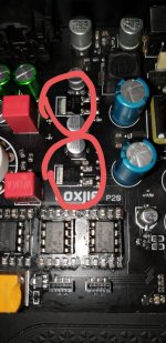
I soldered 4 Op amp sockets to roll op amps on my loxjie p20, I have tried SPARKOS SS3602 but they are all oscillating/making RFI noise.
But with V6 there's wasn't any noise(only slight hiss when turn on amp then all good) but the problem is its rated 16.v but P20s Ref voltage for op amps are 18v, I received an email from Dennis from Burson to confirm if I can use the V6 for long time use, but he said it'll get really hot and told me to use External Fans to cool down the V6.
right now im thinking about reducing the Reference Voltage from 18V to 16.V on P20 so I can use V6 Vivids/Classic opas without worrying about burning them.
Can anyone suggest me whats the best way to reduce the ref Voltage, should I use Voltage Divider using Registors on the sockets? Or is there any other way?
Please suggest me the best way I can reduce the Ref Supply voltage.
Thanks
We would really need to see a circuit diagram to advise. Resistive dividers are not suitable for the currents involved and would in any case ruin what will be a low impedance supply.
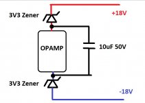
One possible way is to add a Zener diode to each opamp rail per opamp to lose some voltage. Something like a 2.7 or 3.3 volt Zener. You would need suitable decoupling rail to rail across each chip.
Is it really a problem?
Why not measure the current consumption of the Burson at 16 and 18v. It should not actually alter overwide limits and the 2 volts per rail extra won't make much difference at all to power dissipation.
If the power supply has regulators that feed just the opamps then you could look at altering those as another way to do this, whether by changing them for something else or altering their voltage setting components.
The SS3602 datasheet makes it clear the RF decoupling needs to be top-notch, I suspect that P20 lacks proper high-speed decoupling for its opamps. 100nF across the rails ought to do it.
Its odd they didn't just include them on the hybrid itself, I mean that's the obvious place to do it!
Its odd they didn't just include them on the hybrid itself, I mean that's the obvious place to do it!
We would really need to see a circuit diagram to advise. Resistive dividers are not suitable for the currents involved and would in any case ruin what will be a low impedance supply.
One possible way is to add a Zener diode to each opamp rail per opamp to lose some voltage. Something like a 2.7 or 3.3 volt Zener. You would need suitable decoupling rail to rail across each chip.
Is it really a problem?
Why not measure the current consumption of the Burson at 16 and 18v. It should not actually alter overwide limits and the 2 volts per rail extra won't make much difference at all to power dissipation.
If the power supply has regulators that feed just the opamps then you could look at altering those as another way to do this, whether by changing them for something else or altering their voltage setting components.
Hi many Tnx for your interest and sorry for l8 response.
can you pls tell me whats the best zener diode and value to use to reduce the voltage from +18V/-18V to +16V/-16V? and do I need to add extra registors or just the zener diodes from Supply pins to Op Amp pins?
I found two regulators inside but its input pins are at +18/-18V they are only giving 7V output and I'm guessing its for powering tubes, I couldn't trace where exactly the 18V coming from to the supply pins for op amps, I think this Chinese amps design is pretty weird.
I didn't check the output current yet for V5/V6 but I'm assuming the 2V difference wouldn't kill the op amps, The V5i design was influenced by Muses02 op amp and its ABSOLUTE MAX OPERATING VOLTAGE is +-18V and V5i a hybrid op amps so its should able to handle the extra voltage?
I wish Burson Audio was clear about their op amps on their datasheet like sparkos but they are selling their op amps without clean technical explanation which is why people think that their op amps can be used anywhere.
Attachments
Last edited:
The SS3602 datasheet makes it clear the RF decoupling needs to be top-notch, I suspect that P20 lacks proper high-speed decoupling for its opamps. 100nF across the rails ought to do it.
Its odd they didn't just include them on the hybrid itself, I mean that's the obvious place to do it!
I made contact with Andrew from Sparkos OPA and he told me the oscillation occurred for Loxjie P20s PCB design, I think if the SS3602 came with outer case like Bursons V5/V6 opas then the oscillation wouldn't happen.
Well first of all lets put some numbers in...
If the opamp draws say 40 milliamps then if you run it on -/+18 volt you have 1.44 watts dissipation. At -/+16 volt you have 1.28 watts. Its hardly a big increase on what is a fairly large board.
Adding two Zener diodes like this reduces each rail by the value of the Zener, so here you get approx -/+14.7 volt rails. Dissipation would be 1.176 watt in the above example.
The Zeners can be small 0.4 or 0.5 watt types.
Don't forget to add a suitable cap for decoupling as shown.
Attachments
Loxjie P20 ... looking to do similar
Hi, I've also bought a P20 and was looking to part swap the JRC NJM4580 op-amp ...
https://www.njr.com/electronic_device/PDF/NJM4580_E.pdf
with an OPA1612 ...
https://www.ti.com/lit/ds/sbos450c/...69804&ref_url=https%3A%2F%2Fwww.google.com%2F
But, then I read that the op-amps in this design are used for driving the headphones? And the tubes are just used as input buffers?
Does anyone know if that is correct? seems like headphones would like a more current capability and ability to drive lower impedances. TI uses the OPA1622 in this design write up:
https://www.ti.com/lit/ds/symlink/o...37846&ref_url=https%3A%2F%2Fwww.google.com%2F
It is capable of 120mA + output current.
The JRC op amp doesn't seem at all a good choice or capable of driving headphones ... are they really using it at the output? I'd think they'd be using the op-amps for voltage gain at the input and the tubes at the output?
I'll open up my P20 amp and have a look. Anyone here know off hand about this circuit design?
Hi, I've also bought a P20 and was looking to part swap the JRC NJM4580 op-amp ...with an OPA1612 ... But, then I read that the op-amps in this design are used for driving the headphones? And the tubes are just used as input buffers?
Does anyone know if that is correct? seems like headphones would like a more current capability and ability to drive lower impedances. TI uses the OPA1622 in this design write up: It is capable of 120mA + output current.
The JRC op amp doesn't seem at all a good choice or capable of driving headphones ...
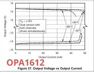
The JRC NJM4580 is a classic for driving headphones, with its 70mA peak ability. The OPA1612 looks like 60mA peak? Yes there are bigger choices but do you really need it?
Tubes a LOW current devices compared to transistors/chips. The 6N3 needs high voltage to touch 7mA (cleanly); 1/10th the current of those chips. The opamps could drive the load +and+ give gain..... but "GLOW!" sells. If the tubes do anything they are a small- or no-voltage gain input.
I was looking at the specs and thinking: it needs 140mA. And maybe 18V (I see 12V). But chips are cheap. Simple enough to series/parallel. In my head I figured 8 opamps, four chips.
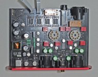
Then I found this gut-shot. The power stage is indeed four chips. The tubes do seem to be wired as something (maybe just cathode-follower?). Then there is a small opamp chip at the input jacks which may do the balancing chores. And logic display or power chips.
Then I found this gut-shot. The power stage is indeed four chips. The tubes do seem to be wired as something (maybe just cathode-follower?). Then there is a small opamp chip at the input jacks which may do the balancing chores. And logic display or power chips.
Attachments
Okay, well that makes more sense … having the opamps in parallel.
The small IC at the input is the digital volume control I suspect.
The tubes do have high voltage , 100 volts , it uses DC to DC converter. It runes hot. I read it is a cathode follower at the input - just a comment on some forum. Anyway, you’re likely correct about it.
The small IC at the input is the digital volume control I suspect.
The tubes do have high voltage , 100 volts , it uses DC to DC converter. It runes hot. I read it is a cathode follower at the input - just a comment on some forum. Anyway, you’re likely correct about it.
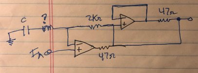
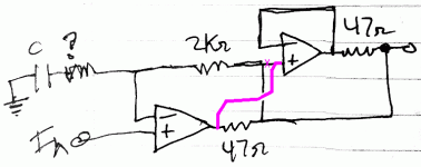
Here is what I’ve come up with so far for the output stage, after some probing.
Not positive about the cap, but would work as a high pass filter. Wasn’t able to get a good reading on the ? resistor because of capacitive coupling. Anyone want to defend this circuit?
The way I see it … I know the input , output and the power supplies. I can remove this opamps and put in my own amplifier design. Probably using the OPA1612.
Attachments
The JRC op amp has big voltage droop with current above 10ma. That’s one reason I prefer the OPA1612. Under load the circuit posted above would multiply the droop issue … with the input of the second op amp buffer being fed by output of the gain op amp which drives the output as well.
Attachments
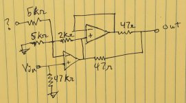
I strongly suggest your circuit is more like this than your drawing.
> big voltage droop with current above 10ma.
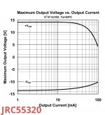
I would call 10% drop "not big", even small. 1dB. The JRC55320 at 10% drop (14V to 12.6V) is flowing 45mA. And 12.6V at 45mA is 280mW at 280 Ohms, VERY LOUD. OTOH, at 100mA we have 5V which supports 250mW in 250 Ohms, not a small sound. Doubled-up we may have 5V 200mA for 500mW in 25 Ohms, and slightly less in 32 Ohms. (The 47 Ohm resistors will modify this especially for low-Z cases.)
Are you actually having trouble getting loud-and-clear? Or just fretting?
> big voltage droop with current above 10ma.
I would call 10% drop "not big", even small. 1dB. The JRC55320 at 10% drop (14V to 12.6V) is flowing 45mA. And 12.6V at 45mA is 280mW at 280 Ohms, VERY LOUD. OTOH, at 100mA we have 5V which supports 250mW in 250 Ohms, not a small sound. Doubled-up we may have 5V 200mA for 500mW in 25 Ohms, and slightly less in 32 Ohms. (The 47 Ohm resistors will modify this especially for low-Z cases.)
Are you actually having trouble getting loud-and-clear? Or just fretting?
Attachments
Yes, you’re correct about the wiring, thanks. I was wondering why the circuit looked different than an application note I saw. I did some more probing tonight and filled in more of the missing pieces.
I’m guessing the question mark is for global feedback to the amp input? Haven’t found where that goes to yet. Any thoughts?
As for what I hear from the stock unit … not very dynamic sounding and lacking some detail. But it is nice sounding and pleasant … certainly well worth the $100 USD spent on it. I bought it with the idea of modding it and have higher expectations for it. I’ll see what I can do with it … I don’t think what I hear is only attributable to the tubes.
Attachments
I tried listening to this amp for the first time with a good DAC, instead of my iPhone. Wow, what a difference. I guess I shouldn't have expected much with my phone. I have just been used to using my phone powering my small P100II Sennheiser headphones, with good results. With the P20 I'm using my HD600 phones.
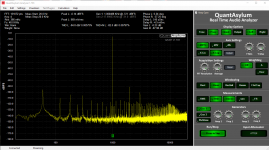
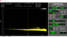
I also took distortion measurements at ~ 1 volt output from the P20 balanced out. I used single ended inputs. See attachments.
It measured about as specified. The right channel looks a bit better in distortion and noise. I'm thinking a difference in tube specs is likely the reason. I also tried putting a 220 ohm resistance load at the output. It made no difference in distortion.
I have a couple 5AH , 12 volt , sealed lead acid batteries. I'm going to use them to power the P20 and see if it helps noise at all. Just want to get a baseline to see if my mods actually make any difference.
Attachments
I also measured the gain of the amp. It was 6 Vout/Vin , so pretty sure that other 5kohm resistor with the ? in front is a feedback resistor. The opamp circuit is set up in a non-inverting topology with a gain of 1.5 for the output voltage from the Tubes. It can also be thought of as summing the feedback voltage and ground (0 volts) at the inverting input, which is just 1/2 the feedback voltage. That's my best guess, but it's clear that the Tubes are providing voltage gain, from what I can see.
Probably didn't explain that well ... but makes sense to me") , the amp input connected to the ? in the circuit diagram would reduce voltage gain of the tubes.
, the amp input connected to the ? in the circuit diagram would reduce voltage gain of the tubes.
Probably didn't explain that well ... but makes sense to me
, the amp input connected to the ? in the circuit diagram would reduce voltage gain of the tubes.- Home
- Amplifiers
- Headphone Systems
- Loxjie P20 OP AMPS Ref Voltage +-18V too high for bursons V6(16.5v)?