I am trying to repair my Linsley Hood designed Class A symetrically driven headphone amp section of my pre-amp that I use as a high level output to my Power amp.
I am guessing that the output transistors are faulty(after over 10 years of use) so have removed them.These are the TIP 41C and TIP 42C(higher rated than the original design which shows TIP 41B and TIP 42B). My Question is,is it important for these output devices to be matched to have close hfe values,particularly as they get quite warm and I assume they would last longer if they shared the output current evenly.If this is important where can I get matched pairs from?
Alternatively I have a lot of quite closely matched(eg-197 hfe PNP/170 hfe NPN) MJE 15034 and MJE 15035 transistors) to hand which have similar specs to the TIP 41C and TIP 42C but slightly lower maximum current and Power ratings(4 Amps,350V,50 Watts as opposed to 6 Amps,100V, 65 Watts) according to the data sheets.Would these be a better alternative?
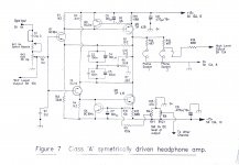
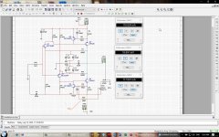
I have attached the schematic that came with the kit for reference.
Any advice much appreciated.
I am guessing that the output transistors are faulty(after over 10 years of use) so have removed them.These are the TIP 41C and TIP 42C(higher rated than the original design which shows TIP 41B and TIP 42B). My Question is,is it important for these output devices to be matched to have close hfe values,particularly as they get quite warm and I assume they would last longer if they shared the output current evenly.If this is important where can I get matched pairs from?
Alternatively I have a lot of quite closely matched(eg-197 hfe PNP/170 hfe NPN) MJE 15034 and MJE 15035 transistors) to hand which have similar specs to the TIP 41C and TIP 42C but slightly lower maximum current and Power ratings(4 Amps,350V,50 Watts as opposed to 6 Amps,100V, 65 Watts) according to the data sheets.Would these be a better alternative?
I have attached the schematic that came with the kit for reference.
Any advice much appreciated.
Attachments
The single positive and single negative output transistors automatically have the same DC bias current.
If paralleled devices for each polarity are used, those should be matched.
You didn't mention the actual problem it has.
Thanks Rayma,One channel would cut out every so often,then eventually there was no music and just a buzz/Hum sounding like mains hum.To complicate the issue,when the channel first cut out I found that the off board power supply to the pre-amp had faulty regulators.I replaced these and the problem came back but only when using the high output from the pre-amp which uses the class A headphone circuit.As the output transistors get quite warm and the problem was initially intermittent,I thought they might be the culprits.Also when looking at the board there were no obvious signs of component damage like bulging caps etc.
After taking out the TIP41C's they measured an hfe gain of 55 and 53 which seems low at least compared to the TIP42C's that measured 187 and 203.
Testing ciruit
Thanks PRR.But before I start what do you mean by Yank R9?
Yank R9. Ground the input. Measure all the key voltages. I've sketched approximate guesses. Yours would be similar, but I expect you will find one/some WAY off. Crayon your readings and post back.
Thanks PRR.But before I start what do you mean by Yank R9?
Measurements compared to ideal
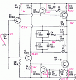
Here are the measurements taken for comparison.The Green are one channel and the blue are the other one.They seem to be pretty close.I don't know whether the 1.5V and 1.47V DC offset at the output is reasonable?If so strange that I couldn't adjust this to lower than 0.77V and 0.69V with the trimpots before temporarily removing the resistors for testing.
Here are the measurements taken for comparison.The Green are one channel and the blue are the other one.They seem to be pretty close.I don't know whether the 1.5V and 1.47V DC offset at the output is reasonable?If so strange that I couldn't adjust this to lower than 0.77V and 0.69V with the trimpots before temporarily removing the resistors for testing.
Attachments
Thanks for the detailed measurements. Something is not balanced but I don't see what. I asked The Idiot to help. First crack gave +0.8V output offset, reasonably close to your observation. So the thing is not inherently zero-centered. And there are some large unbalances. Since my simulated resistors are "exact", the only cause is the inherent difference between NPN and PNP (of similar die-size), which these models obey (a bit too well).
There is a conflict. As Rama observes, Q5 Q6 "must" pass the same current because they are series and there should be no stray DC out of that path. However Q3 Q4 also force Q5 Q6 currents, and not-the-same because Q5 Q6 can not (practically) be exact-matched for both Vbe and hFE.
I added-back the offset trim. It can swing over +/-2.5V at the output. So to get say 10mV offset you have to trim to one part in 500. This is incredibly fine adjustment for a single-turn pot. (Altho not that much finer than an AM radio which must be within 2kHz in a 1MHz band.) It seems that (for these sim parts) the feed to the 10k resistor should be 0.591V for near-zero output offset.
And yet you say it won't pull-in at any setting. Is the voltage *across* RV1 just about 1.44V? But even so, trimming all the way to the negative rail should cause a -negative- output offset, and you only have positive output??
I would wonder about replacing Q1 Q2 just as a mindless way to eliminate possible damage. The biasing should not require high-grade transistors, although hiss and other parameters may suggest types like the ones the Designer specified.
There is a conflict. As Rama observes, Q5 Q6 "must" pass the same current because they are series and there should be no stray DC out of that path. However Q3 Q4 also force Q5 Q6 currents, and not-the-same because Q5 Q6 can not (practically) be exact-matched for both Vbe and hFE.
Someone said a long time ago, in the seventies: "NPN, PNP transistors are as truly matched as men and women of the same height and weight".
I added-back the offset trim. It can swing over +/-2.5V at the output. So to get say 10mV offset you have to trim to one part in 500. This is incredibly fine adjustment for a single-turn pot. (Altho not that much finer than an AM radio which must be within 2kHz in a 1MHz band.) It seems that (for these sim parts) the feed to the 10k resistor should be 0.591V for near-zero output offset.
And yet you say it won't pull-in at any setting. Is the voltage *across* RV1 just about 1.44V? But even so, trimming all the way to the negative rail should cause a -negative- output offset, and you only have positive output??
I would wonder about replacing Q1 Q2 just as a mindless way to eliminate possible damage. The biasing should not require high-grade transistors, although hiss and other parameters may suggest types like the ones the Designer specified.
Attachments
Last edited:
HiHere are the measurements taken for comparison.The Green are one channel and the blue are the other one.They seem to be pretty close.I don't know whether the 1.5V and 1.47V DC offset at the output is reasonable?If so strange that I couldn't adjust this to lower than 0.77V and 0.69V with the trimpots before temporarily removing the resistors for testing.
Don't mind if I give my 5 Cents..
Does the problem Occur on both channels or only one? if its both channels check RAIL VOLTAGE & GROUND otherwise continue to read below.
1. Use a Infrared Thermometer and check the heat of the output Transistors.
Switch on the amp for a minute or two and then point that Thermo Beam against the BLACK BODY of the transistor, not the heat sink.. note down the temp. If it differs more than 20Degrees the one with the higher temp usually has the problem.
2. Here, if the output Transistor have a difference of 100 hfe then I would get the output with balanced equal hfe for both numbers. It doesn't matter if these have 100 or 120 but it's important that they match, say to +- not more than 5
3. about Offset, check that VR both of them.. or the Resistor (47K) which connects to ground that these have full connectivity and the range for 10K does not exceed 10.5k. Check R9 that it reads out 100K, you need to unsolder one side of that one to get a real reading of the Resistor.
4. Last but not least, check for bad soldering spots. *Of course if you have good access to the PCB then you can check for bad solder sots to start with* Ten years for solder is a long time.. Class A tend to get hot, and so sometimes we don't see the small cracks in the solder and when the amp gets hot it disconnects. there I would start with both input transistors.. if sound cuts of and you get hum then usually the Output still connects, otherwise the DC out Measurements would be much higher..
If there everything is OK then Q1 BC184 for leakage..
It also can be anything else, but this would be the major points to look at.
Hope it helps at last.
Last edited:
Thanks for your detailed help PRR. Just checked the voltage across RV1 and it's equivalent on the other channel and it's measuring 1.52V on both.
As you suggest I'll remove Q1 and Q2 and test(I have a peak atlas component analyser) and replace anyway.
hpro-Thanks.I did wonder about matching the hfe of Q5 and Q6,the output transistors,but I understand this is not that important in this kind of design.It's also hard to get hold of matched pairs.
I will however test Q1 with my Peak Atlas analyser but what would indicate leakage?
Last edited:
I think this is not the AMP, but more the PSU
OK. to check BC184 and BC214 is very easy
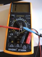
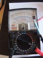
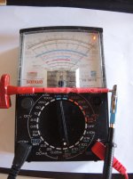
Take if possible a analogue Multi-meter and set it to x1 OHM.
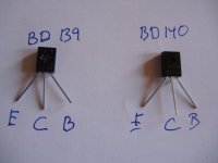
The Transistors I took is just to show how to measure.. The number is not important.This transistors have foot print TO-126
It's important that NPN and PNP must be measured with Reversed Probes to each other.. check out the pics. the same counts for Digital MM and Analogue MM
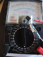
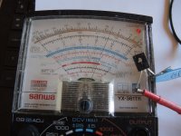
Put the measuring points of the probes together and let the needle go up all the way to O of the Scale. Adjust the needle to 0 OHM on the right side. Picture 1.
Now place the BLACK probe on BASE of the Transistor and the Red on either Emitter or Collector. Pic 2 & 3
Now the Meter should move about 3/4 to right side. the same for Base and Collector. If the needle goes up all the way then the Transistor is bad.
If not good so.
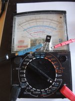
Reverse the Probes, so use the RED PROBE PIN on the BASE * you can check the DATASHEET of BC184 and bc214 which is BASE C and E. Most European Transistors if its TO92 then the base is in the middle.. if its To126 then Base is right, if it's T220 then Base is left. This from the front View where you can read the label of the Transistor.
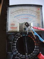
If the needle goes up when measuring with REVERSE the BC184, for both measurements, meaning B-C B-E then you need to Measure E - C and C - E. the needle shouldn't move to the right side.. For the BC214 is to start with Red at the base because this is PNP..
If the needle of the Meter goes near the half of the way on the scale then you need to remove that transistor and measure it out of the circuit. And here is the point.
For BC184 reading good.. No REVERSE READING ALLOWED..See Picture 3&$ this is BD139 also NPN and take a look at the REVERSE PICS as well. If your reading differs of them when the Transistor is out of the PCB then the TRANSISTOR is DEAD or leaks. This measurement is to determine easy if the Transistor still is able to work, while in the PCB
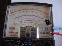
B - C B - E black probe on BASE there the needle 3/4 of the scale OK
Red B - C B - E No movement allowed.. if the needle moves towards right then the Transistor leaks,.
I show you some pictures of Measuring Transistors with a analogue Multi-meter, also the same with a Digital Multi-meter.
Note: Probes for NPN Transistors to measure are reversed to DMM. when measuring a NPN Transistor with analogue then Black Probe goes to BASE using a Digital Multi-meter then RED PROBE goes to base. Reversed for PNPI I doubt that this is the Amp itself.. More likely your Power-supply because both channels showing to much offset. Of the HFE of the Exchanged Transistors are too high.
Does the Power Stage which comes after that Headphone amp, does have a speaker Protection? and does it have a C - in the input Path?
If both yes then even with the C input you will have dropouts because of DC at the Speaker output of the Power Amp.
Check the Supply voltage at that headphone amp that you have the same RAIL VOLTAGES.. May you need to exchange the CAPACITORS in the POWER SUPPLY as well. Check if a VOLTAGE DROP OCCURS at the Headphone amp..
Also note that I used 10K when measuring reverse of the transistors, this means, left side is 100MGOhm or open circuit which for a transistor is good when measured that way.
hope this helps
OK. to check BC184 and BC214 is very easy
Take if possible a analogue Multi-meter and set it to x1 OHM.
The Transistors I took is just to show how to measure.. The number is not important.This transistors have foot print TO-126
It's important that NPN and PNP must be measured with Reversed Probes to each other.. check out the pics. the same counts for Digital MM and Analogue MM
Put the measuring points of the probes together and let the needle go up all the way to O of the Scale. Adjust the needle to 0 OHM on the right side. Picture 1.
Now place the BLACK probe on BASE of the Transistor and the Red on either Emitter or Collector. Pic 2 & 3
Now the Meter should move about 3/4 to right side. the same for Base and Collector. If the needle goes up all the way then the Transistor is bad.
If not good so.
Reverse the Probes, so use the RED PROBE PIN on the BASE * you can check the DATASHEET of BC184 and bc214 which is BASE C and E. Most European Transistors if its TO92 then the base is in the middle.. if its To126 then Base is right, if it's T220 then Base is left. This from the front View where you can read the label of the Transistor.
If the needle goes up when measuring with REVERSE the BC184, for both measurements, meaning B-C B-E then you need to Measure E - C and C - E. the needle shouldn't move to the right side.. For the BC214 is to start with Red at the base because this is PNP..
If the needle of the Meter goes near the half of the way on the scale then you need to remove that transistor and measure it out of the circuit. And here is the point.
For BC184 reading good.. No REVERSE READING ALLOWED..See Picture 3&$ this is BD139 also NPN and take a look at the REVERSE PICS as well. If your reading differs of them when the Transistor is out of the PCB then the TRANSISTOR is DEAD or leaks. This measurement is to determine easy if the Transistor still is able to work, while in the PCB
B - C B - E black probe on BASE there the needle 3/4 of the scale OK
Red B - C B - E No movement allowed.. if the needle moves towards right then the Transistor leaks,.
I show you some pictures of Measuring Transistors with a analogue Multi-meter, also the same with a Digital Multi-meter.
Note: Probes for NPN Transistors to measure are reversed to DMM. when measuring a NPN Transistor with analogue then Black Probe goes to BASE using a Digital Multi-meter then RED PROBE goes to base. Reversed for PNPI I doubt that this is the Amp itself.. More likely your Power-supply because both channels showing to much offset. Of the HFE of the Exchanged Transistors are too high.
Does the Power Stage which comes after that Headphone amp, does have a speaker Protection? and does it have a C - in the input Path?
If both yes then even with the C input you will have dropouts because of DC at the Speaker output of the Power Amp.
Check the Supply voltage at that headphone amp that you have the same RAIL VOLTAGES.. May you need to exchange the CAPACITORS in the POWER SUPPLY as well. Check if a VOLTAGE DROP OCCURS at the Headphone amp..
Also note that I used 10K when measuring reverse of the transistors, this means, left side is 100MGOhm or open circuit which for a transistor is good when measured that way.
hope this helps
Attachments
-
 10. Digital MM Diode reverse measure BD139 - GOOD.jpg265.3 KB · Views: 41
 -
 9.Digital MM Diode measure BD139 - GOOD.jpg234.1 KB · Views: 36
 -
 8.BD140 - Measure BE - Good.jpg266.6 KB · Views: 36
 -
 7.BD140 - Measure BC - GOOD.jpg325.9 KB · Views: 32
 -
 6.BD139-Measure 10k- REVERSE BC open circuit GOOD.jpg312.5 KB · Views: 40
 -
 5.BD139-Measure 1k- REVERSE BC open circuit GOOD.jpg272.4 KB · Views: 99
 -
 4.BD139-measure BE.jpg178.2 KB · Views: 125
 -
 3.BD139-measure BC.jpg175.1 KB · Views: 115
 -
 2 Transistors.jpg148.7 KB · Views: 117
 -
 1. Sanwa 1ohm short.jpg257.4 KB · Views: 108
Last edited:
I've taken out Q1(BC184) and Q2 (BC214) and tested them.They both tested OK with the Peak component Analyzer and I also checked with my multi meter using the diode function and they seemed OK.
I also re-checked the rails and they were just short of 15V:- about -14.75V for negative and +14.75 for positive rail so the Power Supply seems to be OK.
Just one observation:-I noticed it was taking a while for the heatsinks on the output transistors to become warm.Does this mean anything?How long before they should get hot?
Quote:I noticed it was taking a while for the heatsinks on the output transistors to become warm.Does this mean anything?How long before they should get hot?
Is there any HEAT SINK COMPOUND ON the back of these Transistors? If not then get some Silicone Heat sink Compound.. it's better that those Rubber Pads for Class A,,
If heat sink is cold, then heat transfer is to slow and this will heat up the Transistor, and that can be a reason for the OFFSET.
You will need to apply a thin cover of Heat Transfer Compound on the back of the Transistors as well on the heat-sink. Then there should be a MICA and a washer to protect the Transistor against short to the Heat sink.. clean everything well and then apply also on the MICA both sides or on transistor and Heat-sink what comes easier for you..THIS IS A MUST..
Attachments

Last edited:
I see what you are saying hpro there doesn't appear to be much heat even coming straight off the transistors but I can't remember how long they used to take to get hot when they were working properly.I was therefore wondering if the power supply was providing enough current even if the voltage is correct.
What do you think?
What do you think?
OK Let me take a look at the circuit for a few hours.. need to simulate that, to find out what exactly happen.. Hopefully I find it.. here is Swiss we are ahead of your time by one hours.. so check UK time tomorrow morning 10 AM.. then I will know more.
What disturbs me is that both channels have over 1 volt offset.. OK?
enjoy evening ..you hear from me.
What disturbs me is that both channels have over 1 volt offset.. OK?
enjoy evening ..you hear from me.
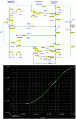
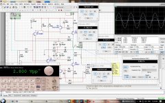
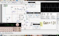
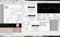
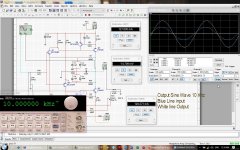
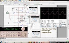
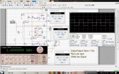
Simulation with National Multisim 14
OK. Lawrence,
as I promised I simulated this amp for you.
All your Measurements, as you got it - and it don't matter if you use TIP41B or C and TIP 42B or C. it's almost the same. TIP42C has less Noise and Amplifies a little bit better..
Gain of this HEADPHONE AMP is 1.3
Frequency Response is 20 - 20 Khz +- 1db. I think this is fair enough.
For me the error would be Resistor 9 = 100k. The resistor is not faulty but I guess it's only 10K and not 100K If I use this resistor with 100K I get DC OUTPUT of about 1.7 to 1.8 Volt and no way to lessen it. may the Schematic has been written the wrong way and the original resistor has been "Streched" this would explain almost everything.
Exchanging this resistor to 10 K then you are able to adjust 0 Volts very easy at about 23% of the Trimpot.. This is your choice. It does not have any influence on sound nor on the output, as the transistor pull only 117.milliamps and that's nothing for a Class A prestage or headphone amp. I do not know what kind of Headphone you are using but you must add 4.7 Ohms to the Headphones Impedance as we have a 4.7 Ohm Resistor in serie with the Headphones.
For the power output it's 11.5 ohms Approximately.
I simulated with only what it used that the amp runs.. as a Headphone AMP
My Resistors are not named in the same manner as yours so please be not surprised.. use the NUMBERS of the circuit you placed online. the value is exactly the same as yours.. and I tested it with both output Transistors..
I do not have BC214 in my Database so I took BC213 it's almost the same. so this also is not a problem because that simulation works exactly as you have measured it..
May PRR can take a look at the Simulation files which I paste here for you and everyone else...
You can only win. 100K resistor: Colors are Brown, Black, Yellow and Gold for 5% Silver for 10%, Red for 2 % and Brown for 1%
10K is Brown, Black, Orange and same as above for the percentage.
Hope this helps.. it's 1 AM here in swiss.. so midnight in England..going to take a nab..
Greetings From Switzerland
Chris Hess
Attachments
-
 7. Headphone amp Distoriton.jpg414.2 KB · Views: 30
 -
 6. Headphone amp Gain.jpg425.3 KB · Views: 31
 -
 5. Headphone amp Sine 20Khz.jpg382.2 KB · Views: 36
 -
 4. Headphone amp Sine 10Khz.jpg382 KB · Views: 27
 -
 3.Headphone Amp.jpg382.8 KB · Views: 33
 -
 2.Headphone Amp.jpg377.8 KB · Views: 42
 -
 1.Headphone Amp.jpg374.2 KB · Views: 49
Hi Chris,
Many thanks for the time you put in to helping me.
I did change the resistor from 100k to 10K and that worked as you said for the DC Offset.Very tricky to get the trim-pot to the right position as has been mentioned by PPR but got it to 20-50mV so a vast improvement.
Unfortunately the left channel dropped out after listening for half hour or so but then came back again so there is still an intermittent fault somewhere.This has happened before.It would drop out cleanly on one channel(no hum or distortion) though sometimes a faint sound before it went completely.Do you have any ideas what may be causing this?
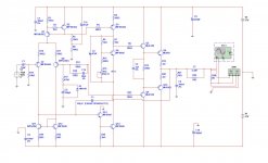
My system is set up so that the Class a headphone amp(within my kit pre-amp) acts as a high output for my power amp which is based on the Doug Self Blamless Amp design(attached). The normal output from the pre-amp is only 500mV which was not enough for the Power amp that requires 1V for full output so this is why I use the higher output from the Headphone stage.
The Power Amp does have protection circuits for the speakers but these don't appear to have been activated when the left channel drops out as they have LED indicators on the front panel to indicate excessive DC at the output.
Many thanks for the time you put in to helping me.
I did change the resistor from 100k to 10K and that worked as you said for the DC Offset.Very tricky to get the trim-pot to the right position as has been mentioned by PPR but got it to 20-50mV so a vast improvement.
Unfortunately the left channel dropped out after listening for half hour or so but then came back again so there is still an intermittent fault somewhere.This has happened before.It would drop out cleanly on one channel(no hum or distortion) though sometimes a faint sound before it went completely.Do you have any ideas what may be causing this?
My system is set up so that the Class a headphone amp(within my kit pre-amp) acts as a high output for my power amp which is based on the Doug Self Blamless Amp design(attached). The normal output from the pre-amp is only 500mV which was not enough for the Power amp that requires 1V for full output so this is why I use the higher output from the Headphone stage.
The Power Amp does have protection circuits for the speakers but these don't appear to have been activated when the left channel drops out as they have LED indicators on the front panel to indicate excessive DC at the output.
Attachments
Last edited:
- Status
- This old topic is closed. If you want to reopen this topic, contact a moderator using the "Report Post" button.
- Home
- Amplifiers
- Headphone Systems
- Reparing Class A symetrically driven Headphone Amp kit